


Fairchild Semiconductor FAN4230 Datasheet
Features at ±5V
• 2.5mA supply current per amplifier
• 358MHz bandwidth
• Output voltage range at RL = 150Ω: -4.9V to 4.81V
• Input includes negative rail
• 217V/µs slew rate
•±130mA output short circuit current
• 12nV/√Hz input voltage noise
• Competes with AD8052 and LMH6643
• Package options (MSOP-8 and SOIC-8)
• Fully specified at +3V, +5V, and ±5V supplies
Applications
• A/D driver
• Active filters
• CCD imaging systems
• CD/DVD ROM
• Coaxial cable drivers
• Portable/battery-powered applications
•Twisted pair driver
•Video driver
Description
The FAN4230 is a dual, low cost, high performance, voltage
feedback amplifier that consumes only 2.5mA of supply current
while providing ±130mAof output short circuit current. The
FAN4230 is designed to operate from 2.5V to 12V (±6V)
supplies. The common mode voltage range extends below the
negative rail and the output provides rail-to-rail performance.
The FAN4230 is designed on a complimentary bipolar
process and provides 358MHz of bandwidth and 217V/µs of
slew rate at a supply voltage of ±5V. The combination of low
power, rail-to-rail performance, low voltage operation, and
tiny package options make the FAN4230 well suited for use
in many general purpose high speed applications.
FAN4230
Dual, High Speed, 2.5V to 12V, Rail-to-Rail Amplifier
www.fairchildsemi.com
Advanced Data September 2003
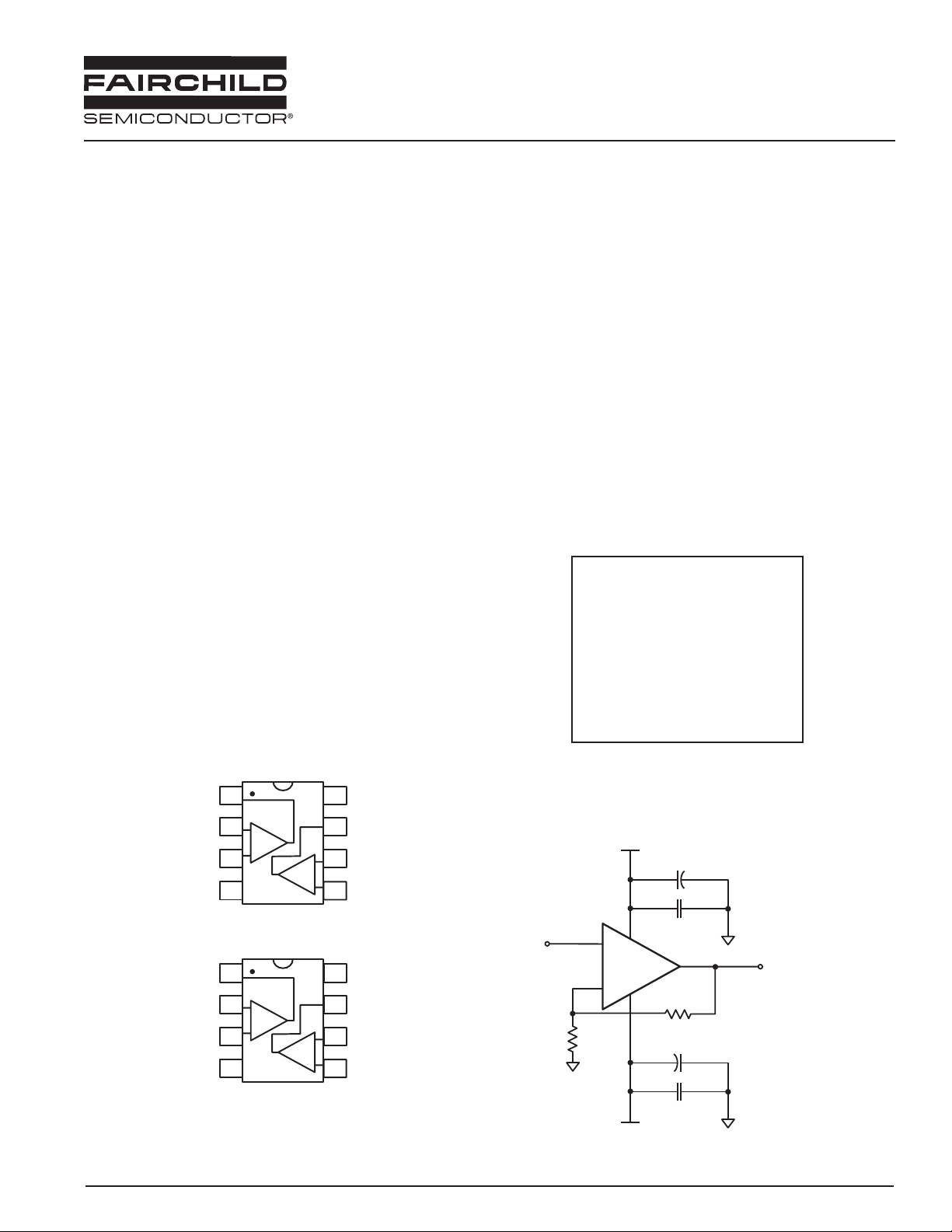
Typical Application
Pin Assignments
ADVANCED DATA
TBD
MSOP
SOIC
-In1
+In1
-V
-In1
+In1
-V
1
2
3
4
s
1
2
3
4
s
Out1
Out1
-
+
-
+
+V
8
s
Out2
7
-In2
6
-
+
5
+In2
+V
8
s
Out2
7
-In2
6
-
+
5
+In2
+V
s
6.8µF
+
+In1
R
g
+
1/2
FAN4230
-
0.01µF
R
f
6.8µF
Out1
+
0.01µF
-V
s
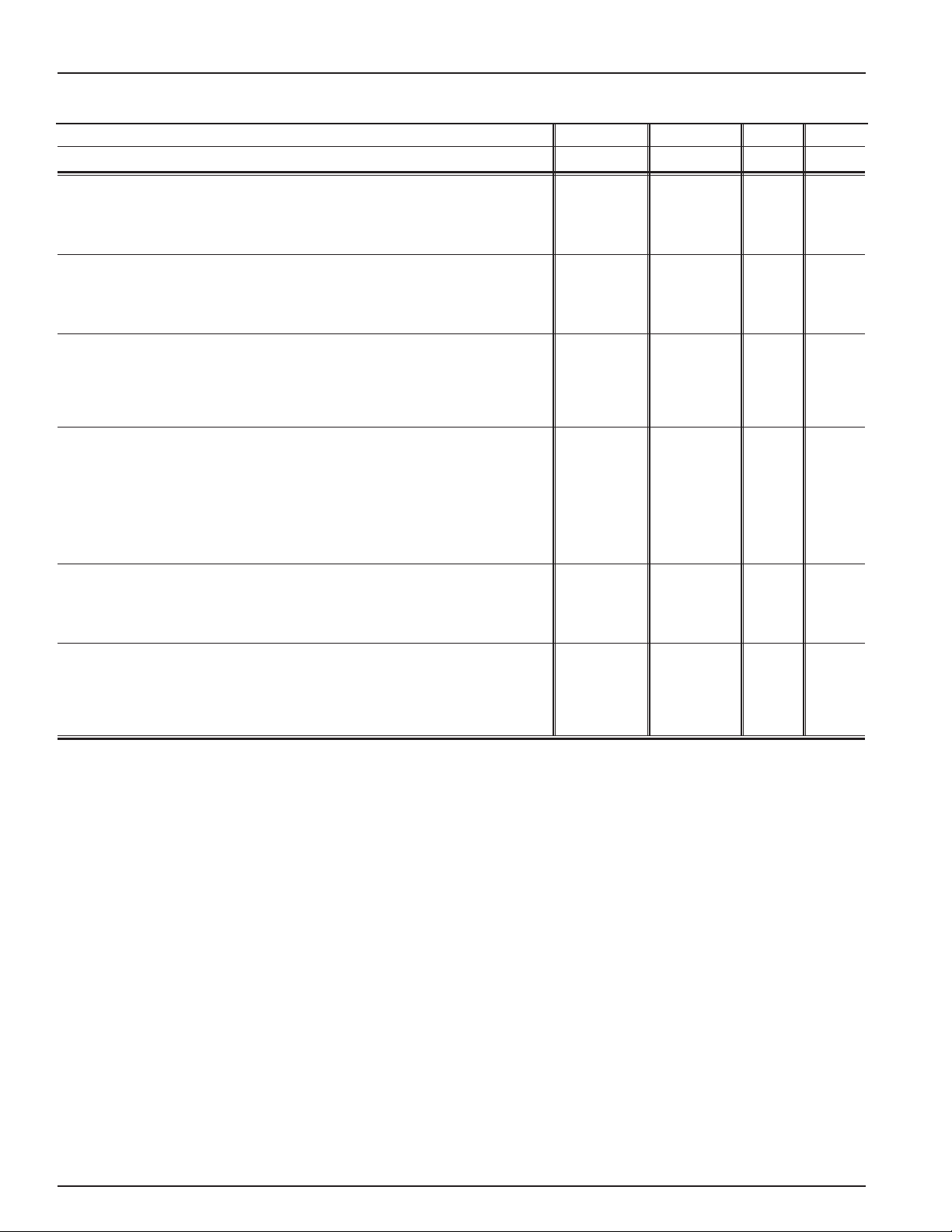
DATA SHEET FAN4230
2 Advanced Data February 2003
Parameters Conditions TYP Min & Max UNITS NOTES
Case Temperature +25°C +25°C
Frequency Domain Response
-3dB bandwidth G = +1, Vo = 0.2V
pp
295 MHz
G = +2, Vo = 0.2V
pp
119 MHz
full power bandwidth G = +2, Vo = 2V
pp
75 MHz
gain bandwidth product 155 MHz
Time Domain Response
rise and fall time 0.2V step 2.74 ns
settling time to 0.1% 2V step TBD ns
overshoot 0.2V step, 8 %
slew rate 3V step, G = -1 215 V/µs
Distortion and Noise Response
2nd harmonic distortion 1Vpp, 5MHz -80 dBc
3rd harmonic distortion 1Vpp, 5MHz -80 dBc
THD 1Vpp, 5MHz 75 dB
input voltage noise >1MHz 12.45 nV/√Hz
crosstalk 10MHz TBD dB
DC Performance
input offset voltage 1 mV 1
average drift TBD µV/°C
input bias current -5 µA1
average drift TBD nA/°C
input offset current TBD µA1
power supply rejection ratio DC 73 dB 1
open loop gain 82 dB 1
quiescent current per amplifier 2.5 mA 1
Input Characteristics
input resistance TBD MΩ
input capacitance TBD pF
input common mode voltage range -0.3 to 1.8 V
common mode rejection ratio DC, V
cm
= 0V to Vs - 1.5 82 dB 1
Output Characteristics
output voltage swing RL = 2kΩ to Vs/2 0.02 to 2.97 V1
RL = 150Ω to Vs/2 0.05 to 2.93 V1
linear output current +99/-99 mA
short circuit output current ±130 mA
power supply operating range 3 2.5 to 12 V
Min/max ratings are based on product characterization and simulation. Individual parameters are tested as noted. Outgoing quality levels
are determined from tested parameters.
NOTES:
1) 100% tested at +25°C.
Electrical Characteristics
(Vs= +3V, G = 2, RL= 2kΩ to Vs/2; unless noted)