

Fairchild Semiconductor FAN2508 Datasheet
www.fairchildsemi.com
FAN2508, FAN2509
50 mA CMOS LDO Regulators
Features
• Ultra Low Power Consumption
• 50 mV dropout voltage at 50 mA
• 25 µA ground current at 50 mA
• Enable/Shutdown Control
• SOT23-5 package
• Thermal limiting
• 300 mA peak current
Applications
• Cellular Phones and accessories
•PDAs
• Portable cameras and video recorders
• Laptop, notebook and palmtop computers
Description
The F AN2508/09 family of micropower lo w-dropout v oltage
regulators utilize CMOS technology to offer a new level of
cost-effective performance in GSM and TDMA cellular
handsets, Laptop and Notebook portable computers, and
other portable devices. Features include extremely low
power consumption and low shutdown current, low dropout
voltage, exceptional loop stability able to accommodate a
wide variety of external capacitors, and the compact SOT23-5
surface-mount package. The F AN2508/09 family of products
offer significant improvements over older BiCMOS designs
and are pin-compatible with many popular devices. The
output is thermally protected against overload.
The FAN2508 and FAN2509 devices are distinguished by
the assignment of pin 4:
FAN2508: pin 4 – ADJ, allowing the user to adjust the
output voltage over a wide range using an external voltage
divider.
FAN2508-XX: pin 4 – BYP, to which a bypass capacitor
may be connected for optimal noise performance. Output
voltage is fixed, indicated by the suffix XX.
FAN2509-XX: pin 4 – ERR
, a flag which indicates that the
output voltage has dropped below the specified minimum
due to a fault condition.
The standard fixed output voltages available are 2.5V, 2.6V,
2.7V, 2.8V , 2.85V, 3.0V , and 3.3V. Custom output voltage are
also available: please contact your local Fairchild Sales
Office for information.
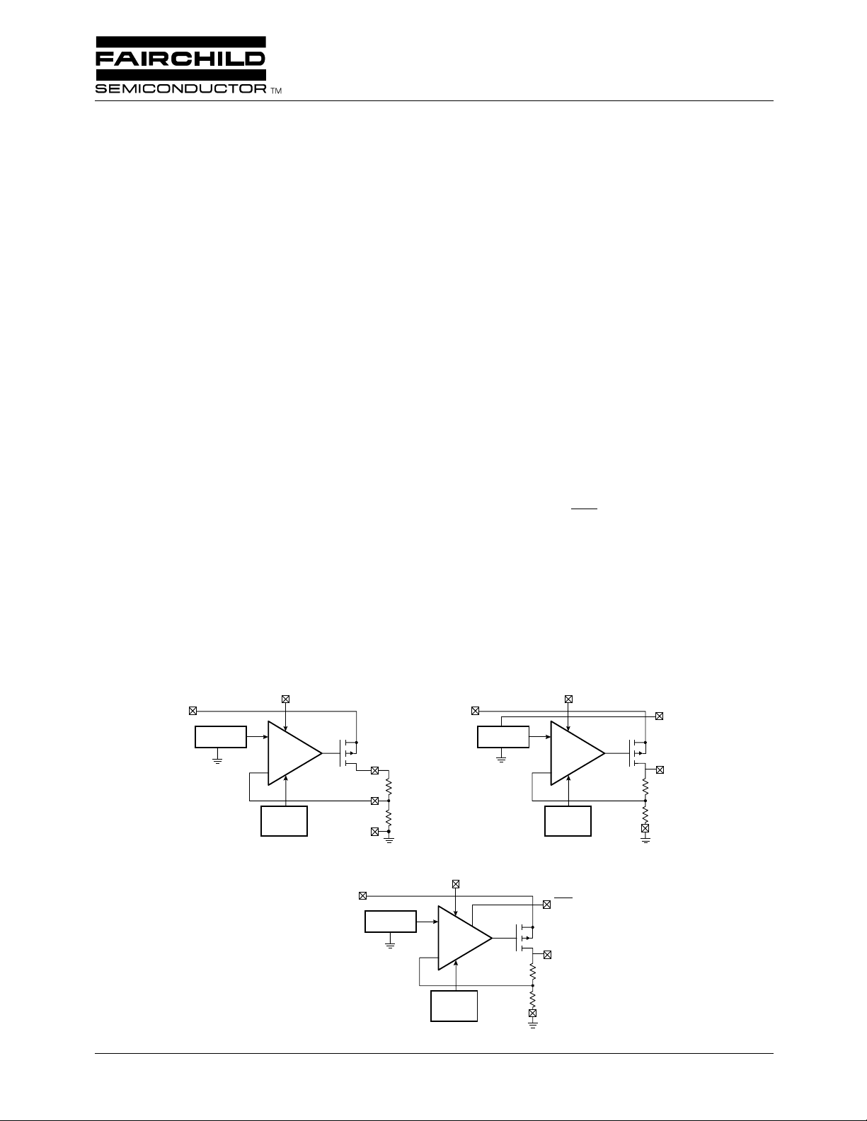
Block Diagrams
V
IN
Bandgap
FAN2508
EN
Error
Amplifier
Thermal
Sense
p
V
IN
FAN2509-XX
V
OUT
ADJ
GND
Bandgap
V
IN
FAN2508-XX
EN
Error
Amplifier
Thermal
Sense
Bandgap
p
Error
Amplifier
Thermal
Sense
ERR
V
OUT
GND
EN
BYP
p
V
OUT
GND
REV. 1.0.6 2/14/03
0:
1:
0:
. 1:
PRODUCT SPECIFICATION FAN2508/FAN2509
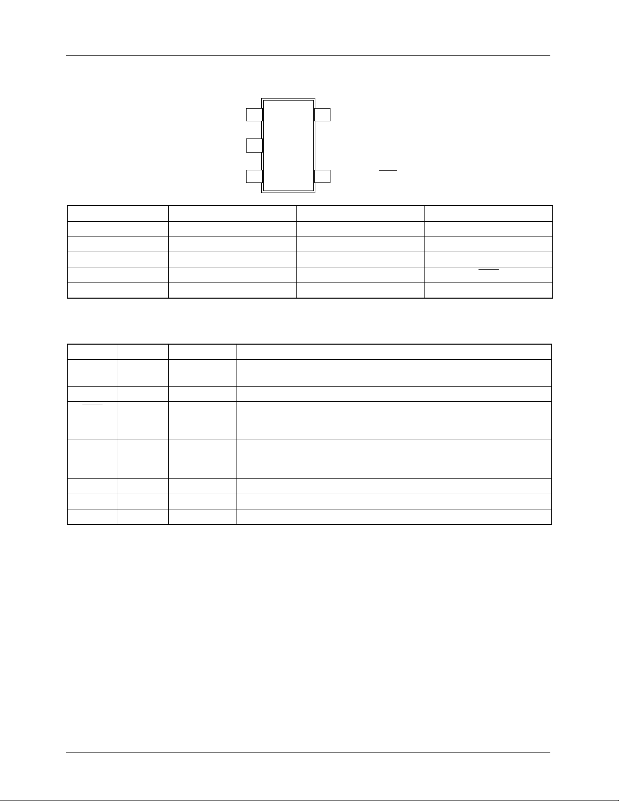
Pin Assignments
15
V
IN
V
OUT
EN
2
3
4
ADJ/BYP/ERR
GND
Pin No. FAN2508 FAN2508-XX FAN2509-XX
1. V
IN
V
IN
2. GND GND GND
3. EN EN EN
4. ADJ BYP ERR
5. V
OUT
V
OUT
Pin Descriptions
Pin Name Pin No. Type Pin Function Description
ADJ 4 Input
BYP 4 Passive
ERR 4 Open drain FAN2509-XX Error. Error flag output.
EN 3 Digital Input Enable.
V
V
IN
OUT
1 Power in
5 Power out
GND 2 Power
FAN2508 Adjust. Ratio of potential divider from VOUT to ADJ
determines output voltage.
FAN2508-XX Bypass. Connect 470 pF capacitor for noise reduction.
Output voltage < 95% of nominal.
Output voltage > 95% of nominal.
Shutdown V
Enable V
OUT
OUT
.
Voltage Input. Supply voltage input.
Voltage Output. Regulated output voltage.
Ground.
V
V
OUT
IN
Functional Description
Designed utilizing CMOS process technology, the
FAN2508/09 family of products are carefully optimized for
use in compact battery-powered devices, offering a unique
combination of low power consumption, extremely low
dropout voltages, high tolerance for a variety of output
capacitors, and the ability to disable the output to less than
1µA under user control. In the circuit, a difference amplifier
controls the current through a series-pass P-Channel
MOSFET, comparing the load voltage at the output with an
onboard low-drift bandgap reference. The series resistance
of the pass P-Channel MOSFET is approximately 1 Ω ,
resulting in an unusually low dropout voltage under load
when compared to older bipolar pass-transistor designs.
2
Protection circuitry is provided onboard for overload conditions. In conditions where the device reaches temperatures
exceeding the specified maximums, an onboard circuit shuts
down the output, where it remains suspended until it has
cooled before re-enabling. The user is also free to shut down
the device using the Enable control pin at any time.
Careful design of the output regulator amplifier assures loop
stability over a wide range of ESR values in the external
output capacitor. A wide range of values and types can be
accomodated, allowing the user to select a capacitor meeting
his space, cost, and performance requirements, and enjoy
reliable operation over temperature, load, and tolerance
variations.
REV. 1.0.6 2/14/03

3
FAN2508/FAN2509 PRODUCT SPECIFICATION
Depending on the model selected, a number of control and
status functions are available to enhance the operation of the
LDO regulator. An Enable pin, available on all devices,
allows the user to shut down the regulator output to conserv e
power, reducing supply current to less than 1µA. The
adjustable-voltage versions of the device utilize pin 4 to
connect to an external voltage divider which feeds back to
the regulator error amplifier, thereby setting the voltage as
desired. Two other functions are available at pin 4 in the
fixed-voltage versions: in noise-sensitive applications, an
external Bypass capacitor connection is provided that allows
the user to achieve optimal noise performance at the output,
while the Error output functions as a diagnostic flag to
indicate that the output voltage has dropped more than 5%
below the nominal fixed voltage.
Applications Information
External Capacitors – Selection
The FAN2508/09 allows the user to utilize a wide variety of
capacitors compared to other LDO products. An innovative
design approach offers significantly reduced sensitivity to
ESR (Effective Series Resistance), which de grades re gulator
loop stability in older designs. While the improvements featured in the FAN2508/09 family greatly simplify the design
task, capacitor quality still must be considered if the designer
is to achieve optimal circuit performance. In general,
ceramic capacitors offer superior ESR performance, at a
lower cost and a smaller case size than tantalums. Those with
X7R or Y5Vdielectric offer the best temperature coefficient
characteristics. The combination of tolerance and variation
over temperature in some capacitor types can result in significant variations, resulting in unstable performance over rated
conditions.
Input Capacitor
An input capacitor of 2.2µF (nominal value) or greater,
connected between the Input pin and Ground, located in
close proximity to the device, will improve transient
response and noise rejection. Higher values will offer superior input ripple rejection and transient response. An input
capacitor is recommended when the input source, either a
battery or a regulated AC voltage, is located far from the
device. Any good quality ceramic, tantalum, or metal film
capacitor will give acceptable performance, however tantalum capacitors with a surge current rating appropriate to the
application must be selected to avoid catastrophic failure.
Output Capacitor
An output capacitor is required to maintain regulator loop
stability. Unlike many other LDO regulators, the
FAN2508/09 family of products are nearly insensitve to
output capacitor ESR. Stable operation will be achieved with
a wide variety of capacitors with ESR values ranging from
10m Ω to 10 Ω or more. Tantalum or aluminum electrolytic,
or multilayer ceramic types can all be used. A nominal v alue
of at least 1µF is recommended.
Bypass Capacitor (FAN2508 Only)
In the fixed-voltage configuration, connecting a capacitor
between the bypass pin and ground can significantly reduce
noise on the output. Values ranging from 470pF to 10nF can
be used, depending on the sensitivity to output noise in the
application.
At the high-impedance Bypass pin, care must be taken in the
circuit layout to minimize noise pickup, and capacitors must
be selected to minimize current loading (leakage). Noise
pickup from external sources can be considerable. Leakage
currents into the Bypass pin will directly affect regulator
accuracy and should be kept as low as possible; thus, highquality ceramic and film types are recommended for their
low leakage characteristics. Cost-sensitive applications not
concerned with noise can omit this capacitor.
Control Functions
Enable Pin
Applying a voltage of 0.4V or less at the Enable pin will
disable the output, reducing the quiescent output current to
less than 1µA, while a voltage of 2.0V or greater will enable
the device. If this shutdown function is not needed, the pin
can simply be connected to the V
float will cause erratic operation.
Error Flag (FAN2509 only)
To indicate conditions such as input voltage dropout
(low V
), overheating, or overloading (e xcessi v e output cur -
IN
rent), the ERR pin indicates a fault condition. It is an opendrain output which is HIGH when the voltage at V
greater than 95% of the nominal rated output voltage and
LOW when V
is less than 95% or the rated output volt-
OUT
age, as specified in the error trip level characteristics.
A logic pullup resistor of 100K Ω is recommended at this
output. The pin can be left disconnected if unused.
Thermal Protection
The F AN2508/09 is designed to supply high peak output cur rents of up to 1A for brief periods, however this output load
will cause the device temperature to increase and exceed
maximum ratings due to power dissipation. During output
overload conditions, when the die temperature exceeds the
shutdown limit temperature of 150°C, onboard thermal
protection will disable the output until the temperature drops
below this limit, at which point the output is then re-enabled.
During a thermal shutdown situation the user may assert the
power-down function at the Enable pin, reducing power
consumption to the minimum level I
pin. Allowing this pin to
IN
OUT
· V
GND
IN
.
is
REV. 1.0.6 2/14/03
 Loading...