

www.fairchildsemi.com
FAN1655
3A DDR Bus Termination Regulator
Features
• Sinks and sources 2.1A continuous, 3A peak
• 0 to +125°C operating temperature range
• 5mA Buffered VREFOUT = VDDQ/2
• Load regulation: VTT = VREFOUT ± 40mV
• On-chip thermal limiting
• Low Cost SO-14, Power Enhanced eTSSOP or
8-pin 5x6mm MLP packages
• Low-Current Shutdown Mode
• Output Short Circuit Protection
Applications
• DDR Terminator VTT supply
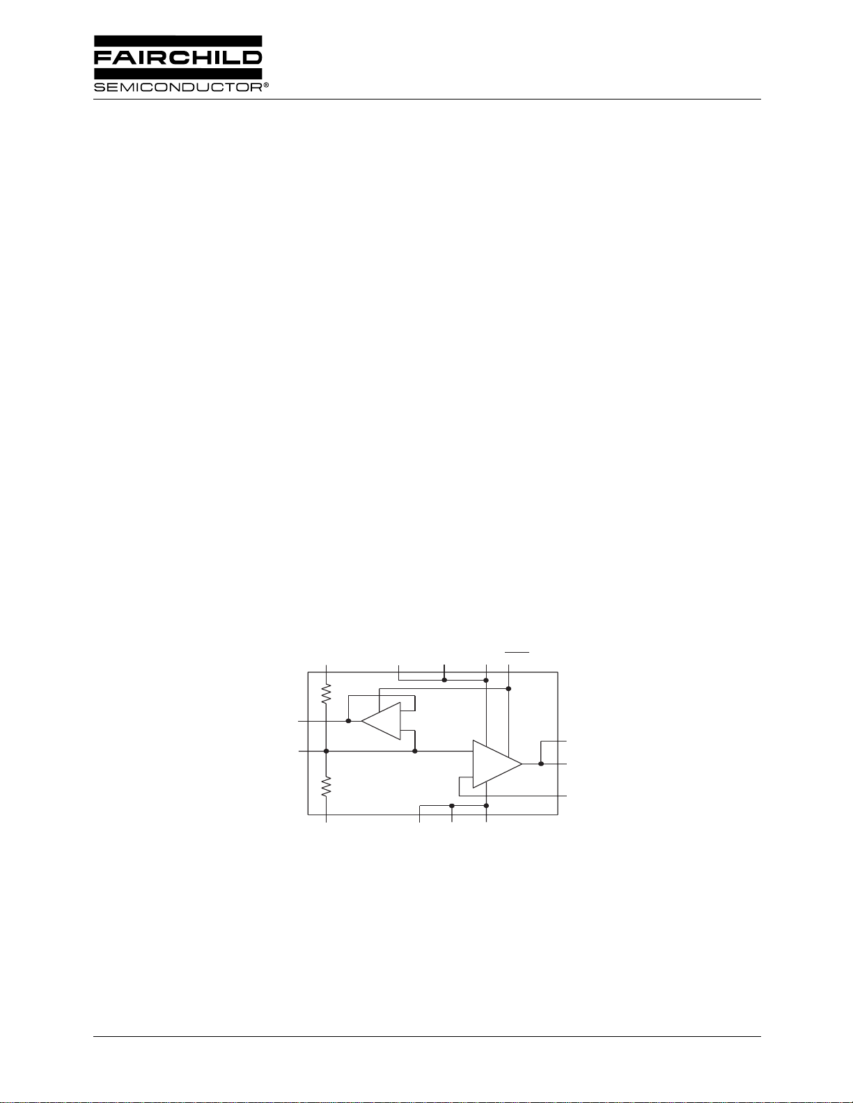
Block Diagram
Description
The FAN1655 is a low-cost bi-directional LDO specifically
designed for terminating DDR memory bus. It can both sink
and source up to 2.1A continuous, 3A peak, providing
enough current for most DDR applications. Load regulation
meets the JEDEC spec, VTT = VREFOUT ± 40mV.
The FAN1655 includes a buffered reference voltage capable
of supplying up to 5mA current. On-chip thermal limiting
provides protection against a combination of power ov erload
and ambient temperature that would create an excessive
junction temperature. A shutdown input puts the FAN1655
into a low power mode.
The FAN1655 regulator is available in a power-enhanced
eTSSOP™-16 package, and the standard SOIC-14
VREFOUT
VREFIN
VDDQ
VSSQ
200k
200k
FAN1655
VDD VDD VDD
-
+
+
-
VSS VSS
VSS
SHDN
VTTFORCE
VTTFORCE
VTTSENSE
REV. 1.1.3 2/20/03

6
5
3
0
9
3
5
6
8
655
C
Q
Q
SHDN
SE
C
CE
SS
SS
CE
SS
3
0
9
8
3
5
6
655M
Q
OUT
Q
SHDN
SE
SS
CE
SS
SS
CE
SHDN
CE
CE
GND
3
6
5
PRODUCT SPECIFICATION FAN1655
Pin Assignments
1
VTTFOR
VTTFOR
N
VDD
1
VREFOUT
V
V
V
FAN1
VSS
1
1
VTTSEN
N
VTTFOR
VTTFOR
V
V
FAN1
VDD
VREF
1
VSS
1
VTTSEN
V
VTTFOR
VTTFOR
8
7
VDDQ
VREFOUT
VTTSENSE
16-Lead Plastic eTSSOP-16
θJC = 4˚C/W*
*With package power slug soldered to 0.5
square inch copper area over backside
ground plane of internal power plane
Pin Definitions
Pin
1, 4 1, 2, 7 1, 2, 7 VDD Input power for the LDO.
2, 3 3, 6 3, 6 VTTFORCE The VTT output voltage.
PAD 4, 5, 8 4, 5, 8 VSS IC Ground.
5 10 9 VTTSENSE Feedback for remote sense of the VTT voltage.
6 12 11 SHDN
7 14 13 VREFOUT Buffered Voltage Reference Output.
8 15 14 VDDQ VDDQ Input. Attach this pin to the VDDQ supply to
11 10 VREFIN Alternative input for direct control of VTTOUT and
13 12 VSSQ Signal Ground.
9, 16 NC No Internal Connection
14-Lead Plastic SOIC
θJC = 37˚C/W, θ
Pin Name Pin Function DescriptionMLP eTSSOP SOIC-14
= 88˚C/W
JA
8-Lead MLP Package (5x6mm)
= 4˚C/W, θ
θ
JC
= 34˚C/W as
JA
measured on FAN1655MP
Eval Board
VREFOUT.
Shutdown. This active low shutdown turns off both VTT
and VREFOUT. This pin has an internal pull-down, and
must be externally driven high for the IC to be on.
generate VTT and VREFOUT.
Typical Application
VDDQ
VDD
VTTFORCE
16
15
14
13
12
11
10
10k
9
1nF
GND
100µF
6V
10µF
1
2
3
4
FAN1655
5
6
7
8
Figure 1. (eTSSOP pinout shown)
2
470µF
10µF
VREFOUT
1nF
SHDN
VTTSENSE
(connect to VTTFORCE
at the load)
GND
REV. 1.1.3 2/20/03

FAN1655 PRODUCT SPECIFICATION
Typical Performance Characteristics
Quiescent Current vs. Temperature
V
REF
7.5
9
1.0
6
0.5
Output Change vs. I
VDD = V
TA = 25˚C
REF
DDQ
= 2.5V
4.5
3
1.5
QUIESCENT CURRENT (mA)
0
-60
-40
-20 0
Figure 2. Quiescent Current vs.
1.260
1.255
1.250
OUTPUT (V)
TT
V
1.245
20
40 60 80
AMBIENT TEMPERATURE (˚C)
Ambient Temperature
100
120
140
(mV)
0
REFOUT
∆ V
-0.5
-1.0
-5
-6
-4 -3
V
REF
Figure 3. Reference Output
Load Regulation
100.0
10.0
Current Pulse Duration (S)
-1 0
-2
LOAD CURRENT (mA)
1
=70°C
T
A
TA=25°C
2
4
3
56
1.240
-3000 -2000 -1000 0 1000 2000 3000
Load Current (mA)
V
TT
Figure 4. V
Load Regulation
TT
REV. 1.1.3 2/20/03
1.0
1 1.5 2 2.5 3
Peak Load Current (A)
Figure 5. Maximum Non-Repetitive Output
Current vs. Pulse Width
(FAN1655M SO-14 Package)
3
 Loading...