

Fairchild Semiconductor DM96L02N Datasheet
March 1989
Revised February 2000
DM96L02
Dual Retriggerable Resettable Monostable Multivibrator
DM96L02 Dual Retriggerable Resettable Monostable Multivibrator
General Description
The DM96L02 is a dual TTL monostab le multivi brator with
trigger mode selection, reset capability, rapid recovery,
internally compensated reference levels and high speed
capability. Output pulse duration and accuracy depend on
external timing co mponents, a nd are the refore und er user
control for each application. It is well suited for a broad variety of applications, including pulse delay generators,
square wave generator s, long del ay time rs, pulse a bsenc e
detectors, frequency de tec tor s, clock pulse generators and
fixed-frequency dividers. Each input is provided with a
clamp diode to limit undershoot and minimize ringing
induced by fast fall times acting on system wiring im pedances.
Features
■ Retriggerable, 0% to 100% duty cycle
■ DC level triggering, insensitive to transition times
■ Leading or trailing-edge triggering
■ Complementary outputs with active pull-ups
■ Pulse width compensation for ∆V
■ 50 ns to ∞ output pulse width range
■ Optional retrigger lock-out capability
■ Resettable, for interrupt operations
CC
and ∆T
A
Ordering Code:
Order Number Package Number Package Description
DM96L02N N16E 16-Lead Plastic Dual-In-Line Package (PDIP), JEDEC MS-001, 0.300 Wide
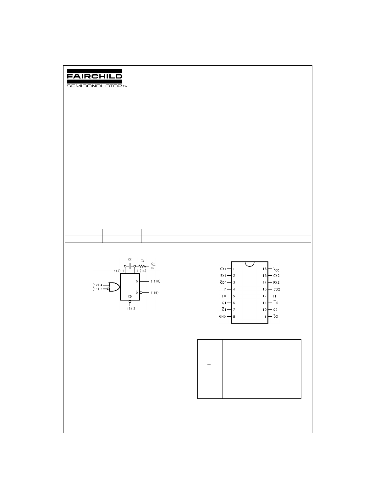
Logic Symbol
Connection Diagram
VCC = Pin 16 GND = Pin 8
Pin Descriptions
Pin Names Description
0 Trigger Input (Active Falling Edge)
I
I1 Trigger Input (Active Rising Edge)
Direct Clear Input (Active LOW)
C
D
Q Positive Pulse Output
Complementary Pulse Output
Q
CX External Capacitor Connection
RX External Resistor Connection
© 2000 Fairchild Semiconductor Corporation DS010203 www.fairchildsemi.com
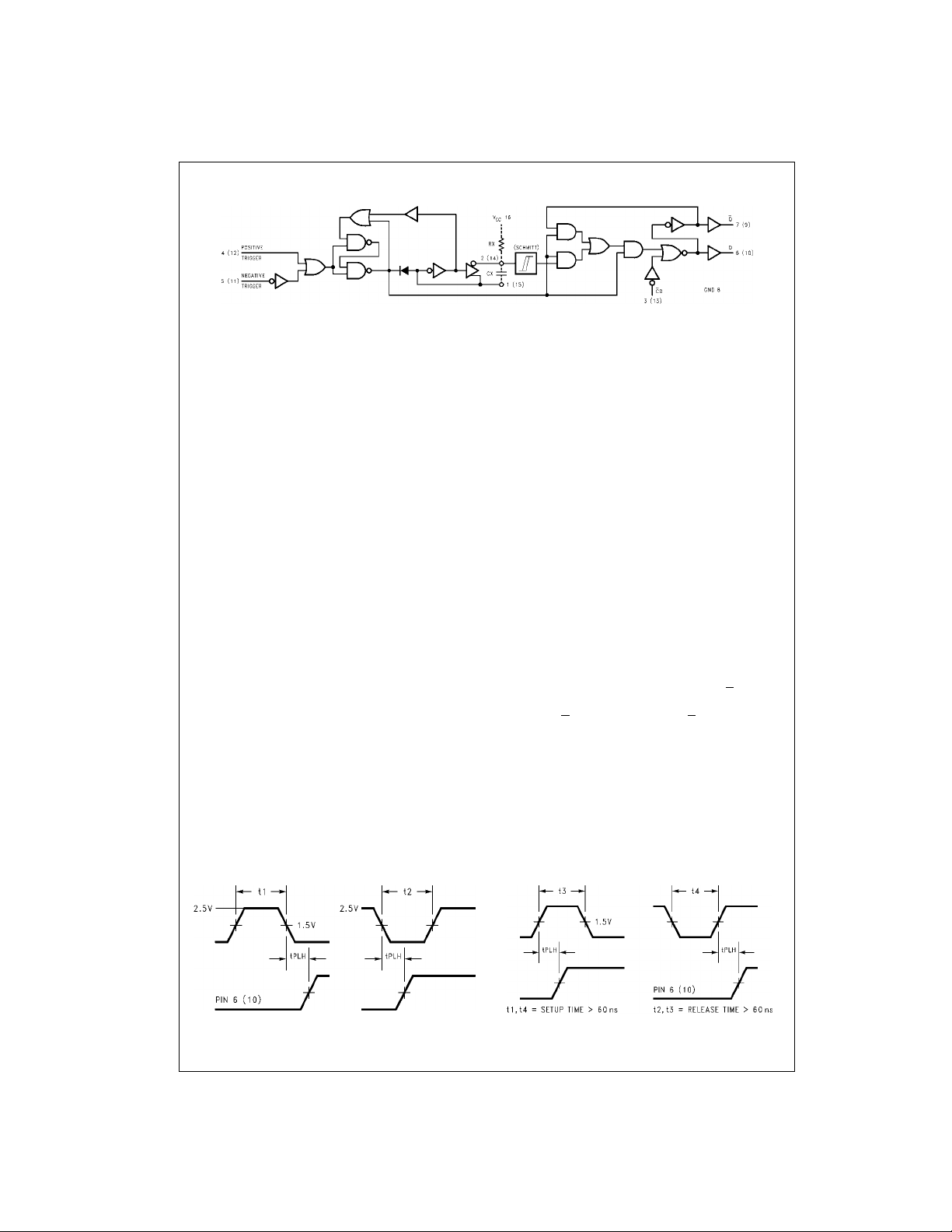
Functional Block Diagram
DM96L02
Operation Notes
1. TRIGGERING—can be accomplished by a positivegoing transition on pin 4 (12) or a negative-going transition on pin 5 (11). Triggering begins as a signal crosses
the input V
internal latch whose unbalanced cross-coupling causes
it to assume a preferred state. As the latch output goes
LOW it disables the gates leading to the Q output and,
through an inverte r, turns on the capacitor discharge
transistor. The inverted signal is also fed back to the
latch input to chan ge its state and effectively end the
triggering action; thus the latch and its associated feedback perform the function of a differentiator.
The emitters of the latch tr ansistors return to ground
through an enabling transistor which must be turned off
between successive triggers in order for the latch to
proceed through th e proper sequence when triggering
is desired. Pin 5 ( 11) must be HIGH in order to tr igger
at pin 4 (12); conve rsely, pin 4 (12) must b e LOW in
order to tri gger at pin 5 (11).
2. RETRIGGERING—In a normal cycle, triggering initiates a rapid discharge of the external timing capacitor,
followed by a ram p voltage run-up at pin 2 (14). The
delay will time out when the ramp voltage reaches the
upper trigger point of a Schmitt circuit, causing the outputs to revert to the quiescent s tate. If another trigger
occurs before the ramp voltage reaches the Schmitt
threshold, the capacitor will be discharged and the
ramp will start again without having disturbed the output. The delay per i od c an t herefore be extended fo r a n
arbitrary length of time by insuring that the interval
between triggers is less than the de lay time, as de termined by the external capacitor and resistor.
3. NON-RETRIGGERABLE OPERATION—Retriggering
can be inhibited logically, by connecting pin 6 (10) back
to pin 4 (12) or by conne cting pin 7 (9) back to pin 5
(11). Either hook-up has the effect of keeping the latchenabling transistor turned on during the delay period,
which prevents the input latch from cycling as discussed above in the section on triggering.
threshold region; this activates an
IL:VIH
4. OUTPUT PULSE WIDTH—An external resistor R
an external capacitor C
are required, a s shown in the
X
X
and
functional block diagram. To minimize stray capacitance and noise pickup, R
and CX should be located
X
as close as possible to the circuit. In applications which
require remote trimming of the pulse width, as with a
variable resistor, R
should consist of a fixed resistor in
X
series with the variable resistor; the fixed resistor
should be located as close as po ssible to the circuit.
The output pulse w idth t
is in kΩ, CX is in pF and tW is in ns.
R
X
= 0.33 RXCX (1 + 3/RX) for CX ≥ 103 pF
t
W
16 kΩ ≤ R
20 kΩ ≤ R
C
C
≤ 220 kΩ for 0°C to +75°C
X
≤ 100 kΩ for −55°C to +125°C
X
may vary from 0 to any value. For pulse wid ths wit h
X
less than 103 pF see Figure 1.
X
is defined as follows, where
W
5. SETUP AND RELEASE TIMES—The setup times
listed below are necessary to allow the latch-enabling
transistor to turn o ff and the node voltages wit hin the
input latch to stabilize , thus insuring proper cycling of
the latch when the next trigger occurs. The indica ted
release times (equivalent to trigger duration) allow time
for the input latch to cycle and its signal to propagate.
6. RESET OPERATION—A LOW signal on C
, pin 3
D
(13), will terminate an output pulse, causing Q to go
LOW and Q
to go HIGH. As long as CD is held LOW, a
delay period cannot be initiated nor will attempted triggering cause spikes at th e o utp uts. A reset pulse duration, in the LOW state, of 25 ns is sufficient to insure
resetting. If the reset input goes LOW at the same time
that a trigger transition occurs, the reset will dominate
and the outputs will not respond to the trigger. If the
reset input goes HIGH coincident with a trigger transition, the circuit will respond to the trigger.
Input to Pin 5 (11) Pin 4 (12) = L Pin 3 (13) = H
www.fairchildsemi.com 2
Input to Pin 4 (12) Pins 5 (11) and 3 (13) = H
 Loading...