Fairchild Semiconductor DM9602N, DM9602CW Datasheet

© 2000 Fairchild Semiconductor Corporation DS006611 www.fairchildsemi.com
August 1986
Revised February 2000
DM9602 Dual Retriggerable, Resettable One Shots
DM9602
Dual Retriggerable, Resettable One Shots
General Description
These dual resettable, retrig gerable one shots have two
inputs per function; one which is active HIGH, and one
which is active LOW. This allows the de signer to employ
either leading-edge or trailing-edge triggering, which is
independent of input transition times. When input conditions for triggering are met, a new cycle starts and the
external capacitor is allowe d to rapidl y discharge an d then
charge again. The retriggerable feature permits output
pulse widths to be extended. In fact a con tinuous true ou tput can be maintained by having an input cycl e time whi ch
is shorter than the output cycle time. The ou tpu t pulse may
then be terminated at any tim e by applying a LOW logic
level to the RESET pin . Retriggering may be i nhibited by
either connecting the Q output to an active HIGH input, or
the Q
output to an active LOW input.
Features
■ 70 ns to ∞ output width range
■ Resettable and retriggerable—0% to 100% duty cycle
■ TTL input gating—leading or trailing edge triggering
■ Complementary TTL outputs
■ Optional retrigger lock-out capability
■ Pulse width compensated for V
CC
and temperature vari-
ations
Ordering Code:
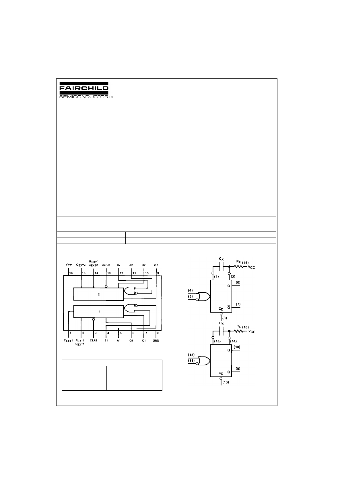
Connection Diagram
Function Table
H = HIGH Voltage Level
L = LOW Voltage Level
X = Don’t Care
Logic Diagrams
Order Number Package Number Package Description
DM9602N N16E 16-Lead Plastic Dual-In-Line Package (PDIP), JEDEC MS-001, 0.300 Wide
Pin Numbers
Operation
ABCLR
H→L L H Trigger
HL→H H Trigger
XXL Reset

www.fairchildsemi.com 2
DM9602
Operating Rules
1. An external resistor (RX) and external capacito r (CX)
are required as shown in the Logic Diagram.
2. The value of C
X
may vary from 0 to any necessary
value available. If, however, the capacitor has leakages
approaching 3.0 µA or if stray capacitance from either
terminal to ground is more than 50 pF, the timing equations may not represent the pulse width obtained.
3. The output pulse with (t) is defined as follows:
where: R
X
is in kΩ, CX is in pF
t is in ns
for C
X
< 103 pF, see Figure 1.
for K vs. C
X
see Figure 6.
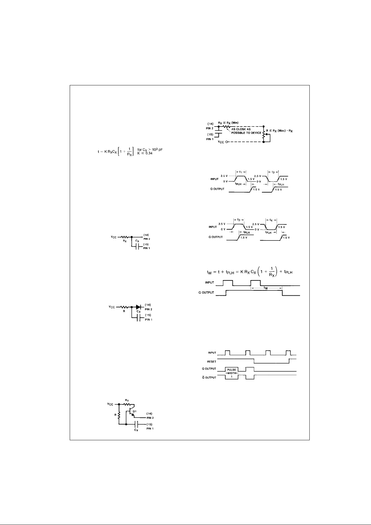
4. If electrolytic type capacitors are to be used, the following three configurations are recommended:
1. Use with low leakage capacitors:
The normal RC con figuration can b e used pred ictably only if the forward capacitor leakage at 5.0V is
less than 3 µA, and the inve rse capacitor l eakage
at 1.0V is less than 5 µA over the operational temperature range.
R < 0.6 RX (Max)
2. Use with high inver se leakage current electrolytic
capacitors:
The diode in this configuration prevents high
inverse leakage curr ents through the capacitor by
preventing an inver se vo l tag e a cross the capacitor.
The use of this config uration is not recomme nded
with retriggerable operation.
t ≈ 0.3 RC
X
3. Use to obtain extended pulse widths:
This configuration ca n be used to obtain exte nded
pulse widths, b ecause of the larger timing r esistor
allowed by beta multiplication. Electrolytics with
high inverse leakage currents can be used.
R < R
X
(0.7) (hFE Q1) or < 2.5 MΩ, whichever is the
lesser
R
X
(min) < RY < RX (max)
(5 kΩ ≤ R
Y
≤ 10 kΩ is recommended)
Q1: NPN silicon transistor with h
FE
requirements of
above equations, such as 2N5961 or 2N5962.
t ≈ 0.3 RC
X
This configuration is no t recommend ed with retrigg erable ope ration.
5. To obtain variable pulse width by remote trimming, the
following circuit is recommended:
6. Under any opera ting condition, C
X
and RX (min) must
be kept as close to the circ uit as possible to min imize
stray capacitance and reduce noise pickup.
7. Input Trigger Pulse Rules (See Triggering Truth Table)
Input to Pin 5(11), (Pin 3(13) = HIGH)
Pin 4(12) = LOW
t
1
, t3 = Min. Positive Input Pulse Width > 40 ns
t
2
, t4 = Min. Negative Input Pulse Width > 40 ns
Input to Pin 4(12) (Pin 3(13) = HIGH)
Pin 5(11) = HIGH
8. The retriggerable pulse width is calculated as shown
below:
The retrigger pu lse width is e qual to the pulse widt h (t) plus a d elay
time. For pulse widths greater than 500 ns, t
W
can be approximated as
t. Retriggering wil l not occu r if the retrigger p ulse come s within ≈ 0.3
C
X
(ns) after the initial trig ger pulse (i.e., during th e discharge cycle).
9. Reset Operation—An overriding clear (active LOW
level) is provided on each one shot. By applying a LOW
to the reset, any timing cy cle can be termi nated or any
new cycle inhibited until the LOW reset input is
removed. Trigger inputs will not produce spikes in the
output when the reset is held LOW.
10. V
CC
and Ground wir ing should conform to g ood high
frequency standards so that switching transients on
V
CC
and Ground leads do not cause interaction
between one shots. Us e of a 0.01 to 0.1 µF bypass
capacitor between V
CC
and Ground locat ed near the
DM9602 is recommended.
Note 1: For further detailed device ch aracteristics and outp ut performance,
please refer to the NSC one-shot application note, AN-366.
