Fairchild Semiconductor DM93S62N Datasheet

October 1988
Revised May 2000
DM93S62
9-Input Parity Checker/Generator
General Description
The DM93S62 is a ve ry high speed 9 -input pari ty checke r/
generator for use in error detection and error correction
applications. The DM93S 62 provides odd and even parity
for up to nine data bits. The even parity output (PE) is
HIGH if an even number of inputs are HIGH and E
The odd parity output (PO) will be HIGH if a n odd number
of inputs are HIGH and E
Enable (E
) input forces both outputs LOW.
is LOW. A HIGH level on the
Ordering Code:
Order Number Package Number Package Description
DM93S62N N14A 14-Lead Plastic Dual-In-Line Package (PDIP), JEDEC MS-001, 0.300 Wide
is LOW.
DM93S62 9-Input Parity Checker/Generator
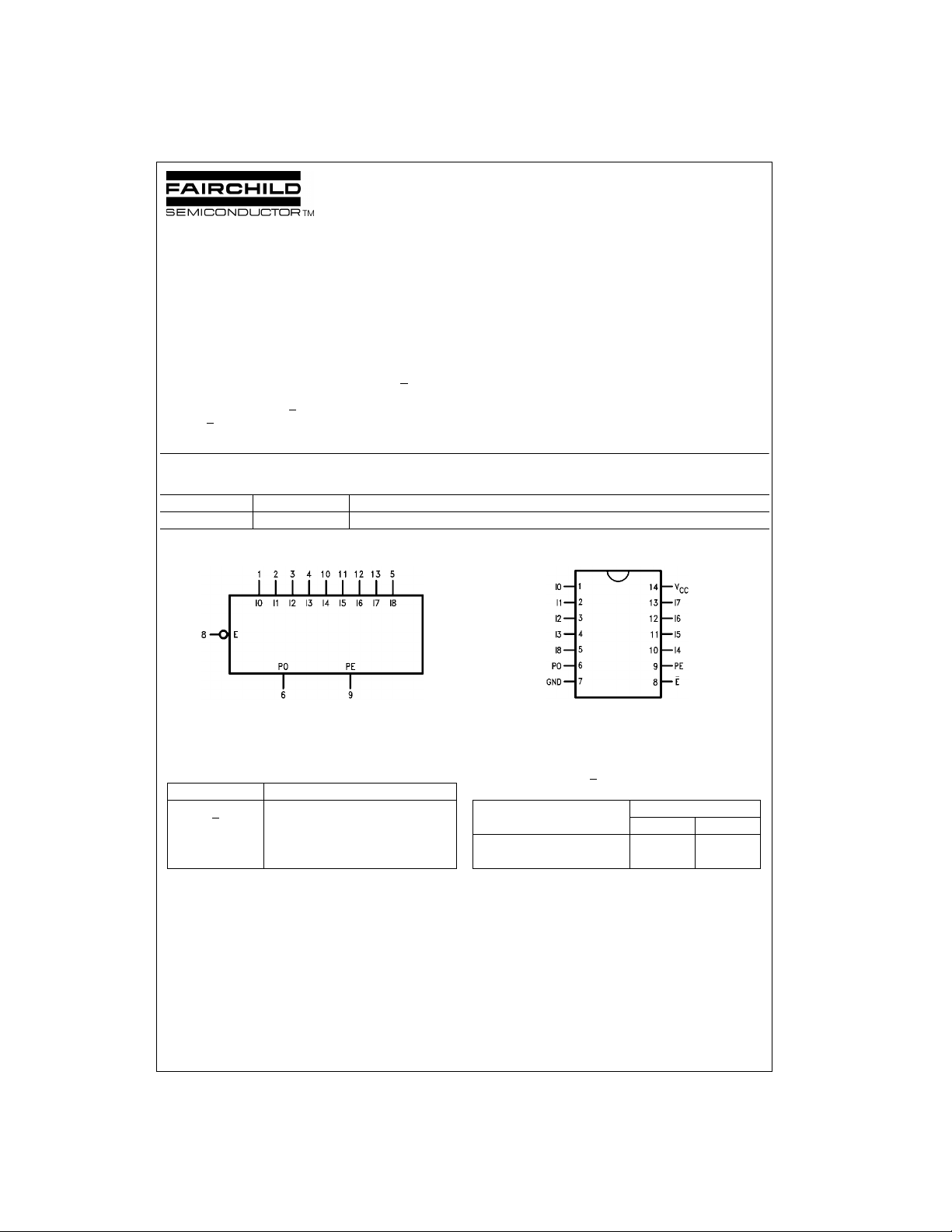
Logic Symbol
VCC = Pin 14
GND = Pin 7
Connection Diagram
Pin Descriptions Truth Table
Pin Name Description
I0–I8 Data Inputs
E Output Enable (Active LOW)
PO Odd Parity Output
PE Even Parity Output
Number of Inputs Outputs
I0–I8 that are HIGH PO PE
1, 3, 5, 7, 9 H L
0, 2, 4, 6, 8 L H
H = HIGH Voltage Level
L = LOW Voltage Level
(E = LOW)
© 2000 Fairchild Semiconductor Corporation DS009809 www.fairchildsemi.com

Functional Description
The DM93S62 is a very h igh speed 9-inpu t parity checker
or generator. It is intended primarily for error detection in
systems which trans mit data in 8-bit bytes, but it can be
DM93S62
expanded to any number of data inputs. Both even and odd
parity outputs are available to al low maximu m flexibility for
both parity generation and parity checking. When the
device is enabled (E
is HIGH when an even number of inpu ts is HIG H, and th e
Odd Parity output (PO) is HIGH when an odd number of
inputs is HIGH. The active LOW Enable (E
state of both outputs; when the Enable (E
outputs will be LOW. The Enable may be used to strobe the
outputs at very high speeds to synchronize or inhibit the
parity data.
The DM93S62 has been designed with two sections using
Exclusive-NOR comparison techniques. Eigh t data inputs
= LOW ), the Even Par ity output (PE)
) controls the
) is HIGH, both
TABLE 1. Termination Recommendations for Less than Nine Bits
Number of I0 I1 I2 I3 I4 I5 I6 I7 I8
Data Inputs
3 D0LD1LD2L L L L
4 D0LD1LD2LD3L L
5 D0LD1LD2LD3LD4
6 D0D1D2D3D4 L D5 L L
7 D0D1D2D3D4 L D5 L D6
8 D0D1D2D3D4D5D6D7 L
I0–I7 represent one section which will generate a parity bit
in 16 ns to 20 ns. The ninth input (I8) bypasses three levels
of logic and switches the o utputs in 6.0 ns to 9.0 ns. This
feature may be used t o compensate for d elayed arrival of
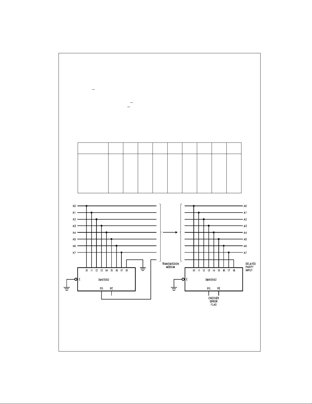
the parity bit, allowing faster system cycle times (Figure 1).
The fast I8 input is also useful when more than nine bits
are to be checked. Th e outp ut of o ne DM93S62 driv es the
I8 input of a second DM93 S62, providing a 17-bit parity
check in 29 ns (typ).
When some inputs of the DM93S 62 are not used , such as
for words of less than nine bits or when using parallel
expansion techniqu es, there is an optimu m delay scheme
for termination of the unused inputs (see Table 1). In
essence, if one of the in puts of any Exclusive -NOR stays
HIGH, the delay from the other input to the output is minimized.
FIGURE 1. Fast Input I8 allows Higher System Speed
www.fairchildsemi.com 2
 Loading...