

Fairchild Semiconductor DM93S41N Datasheet
October 1988
Revised May 2000
DM93S41
4-Bit Arithmetic Logic Unit
General Description
The DM93S41 4-bit arithm etic logic units can perform all
the possible 16 logic operations on two variables and a
variety of arithmetic operations; the Add and Subtract
modes are the most important.
Ordering Code:
Order Number Package Number Package Description
DM93S41N N24A 24-Lead Plastic Dual-In-Line Package (PDIP), JEDEC MS-010, 0.600 Wide
DM93S41 4-Bit Arithmetic Logic Unit
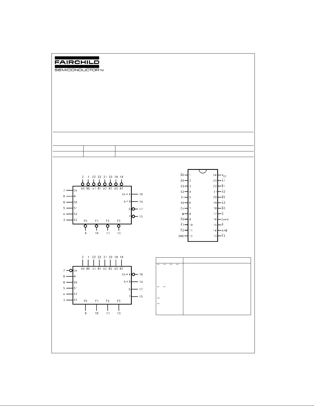
Logic Symbols
Active LOW Operands
Active HIGH Operands
Connection Diagram
Pin Descriptions
Pin Name Description
A
0–A3, B0–B3 Operand Inputs (Active LOW)
S0–S3 Function Select Inputs
M Mode Contr ol Input
Cn Carry Input
F
0–F3 Function Outputs (Active LOW)
A = B Comparator Output
G Carry Generate Output (Active LOW)
P
C
n+4
Carry Propagate Output (Active LOW)
Carry Output
© 2000 Fairchild Semiconductor Corporation DS009805 www.fairchildsemi.com
Functional Description
The DM93S41 is a 4-bit high speed parallel arithmetic logic
unit (ALU). Contro lled by the four Function Select inputs
(S0–S3) and the Mode Contro l inpu t (M), i t can p erform all
DM93S41
the 16 possible op era tion s or 1 6 d ifferent arithmetic op era tions on active HIGH or active LOW operands. The Function Table below lists these operations.
When the Mode Control input (M) is HIGH, all internal carries are inhibited and the device p erforms logic oper ations
on the individual bits as listed. When the Mode Control
input is LOW, the carries are enabled and the dev ice performs arithmetic operations on the two 4-bit words. The
device incorporates full internal carry lookahead and provides for either ripple carry between devices using the C
output, or for carry lookahead between packages using the
signals P
(Carry Propagate) and G (Carry Generate). P
and G are not affected by carry in. When spe ed requirements are not string ent, the DM93S41 can be used in a
simple ripple carry mode by connecting the Carry output
(C
) signal to the Carry i nput (Cn) of the next unit. For
n+4
super high speed oper atio n the Schot tky DM9 3S41 shou ld
be used in conjunction with the '42 carry lookahead circuit.
The A = B output from the DM93S41 goes HIGH when all
outputs are HIGH and can be used to indicate logic
four F
n
equivalence over four bits when the u nit is in the subtr act
mode. The A = B output is open-collector and can be wiredAND with the other A = B outputs to give a comparison for
more than four bits. The A = B signal can also be used with
the C
signal to indicate A > B and A < B.
n+4
The Function Table lists the arithmetic ope rations that are
performed without a carry in. An incoming carry adds a one
to each operation. Thus select code LHHL generates A
minus B minus 1 (2s complem ent no tation) witho ut a ca rry
in and generates A minus B when a carry is applied.
n+4
Because subtraction is actu ally performed by co mplementary addition (1s complemen t), a carry out mea ns borrow;
thus a carry is gener ated when there i s no underflow and
no carry is generated when there is underflow.
As indicated the '41 can be used with either active LO W
inputs producing active LOW outputs or with active HIGH
inputs producing active HIGH outp uts. For either case the
table lists the operatio ns that are performed to the ope rands labeled inside the logic symbol.
Function Table
Mode Select Active LOW Inputs Active HIGH Inputs
Inputs & Outputs & Outputs
Logic Arithmetic (Note 2) Logic Arithmetic (Note 2)
S3 S2 S1 S0 (M = H) (M = L) (C
LLLLA
LLLHAB
LLHLA
+ B AB minus 1 ABA + B
A minus 1 A A
AB minus 1 A + B A + B
L L H H Logic 1 minus 1 Logic 0 minus 1
LHLLA
+ B A plus (A + B)ABA plus AB
LHLHB AB plus (A + B)B (A +B) plus AB
LHHLA ⊕ B A minus B minus 1 A ⊕ B A minus B minus 1
LHHHA + B
HLLLA
BA plus (A + B) A + B A plus AB
A + B AB AB minus 1
HLLHA ⊕ B A plus B A ⊕ B A plus B
HLHLB AB
plus (A + B) B (A + B) plus AB
HLHHA + BA + B AB AB minus 1
H H L L Logic 0 A plus A (Note 1) Logic 1 A plus A (Note 1)
HHLHAB
H H H L AB AB
AB plus A A + B (A + B) plus A
minus A A + B(A + B) plus A
HHHHAA AA minus 1
H = HIGH Voltage Level
L = LOW Voltage Level
Note 1: Each bit is shifted to the next more significant position
Note 2: Arithmetic operations ex pressed in 2s complement notation
= L) (M = H) (M = L) (Cn = H)
n
www.fairchildsemi.com 2
Symbol
t
PLH
t
PLH
t
PLH
t
PLH
t
PLH
t
PLH
t
PLH
t
PLH
t
PLH
t
PLH
t
PLH
Symbol
t
PLH
t
PLH
t
PLH
t
PLH
t
PLH
t
PLH
t
PLH
t
PLH
t
PLH
t
PLH
t
PLH
t
PLH
t
PLH
Symbol
t
PLH
t
PLH
DM93S41
TABLE 1. SUM MODE TEST Function Inputs: S0 = S3 = 4.5V, S1 = S2 = M = 0V
Input Other Input Same Bit Other Data Input Output
Under Apply Apply Apply Apply Under
Test 4.5V GND 4.5V GND Test
, t
PHL
, t
PHL
, t
PHL
, t
PHL
, t
PHL
, t
PHL
, t
PHL
, t
PHL
, t
PHL
, t
PHL
, t
PHL
, t
PHL
, t
PHL
, t
PHL
, t
PHL
, t
PHL
, t
PHL
, t
PHL
, t
PHL
, t
PHL
, t
PHL
, t
PHL
, t
PHL
, t
PHL
, t
PHL
, t
PHL
A
i
B
i
A
i
B
i
A B None None Remaining A and B, C
B A None None Remaining A and B, C
A None B Remaining B Remaining A, C
B None A Remaining B Remaining A, C
A None B Remaining B Remaining A, C
B None A Remaining B Remaining A, C
C
n
B
i
A
i
B
i
A
i
None Remaining A to B C
None Remaining A to B C
None C
None C
n
n
Remaining A and B F
Remaining A and B F
n
n
n
n
n
n
n
n
F
i
F
i
i + 1
i + 1
P
P
G
G
C
n + 4
C
n + 4
None None All A All B Any F or C
TABLE 2. DIFF MODE TEST Function Inputs: S1 = S2 = 4.5V,S0 = S3 = M = 0V
Input Other Input Same Bit Other Data Inputs Output
Under Apply Apply Apply Apply Under
Test 4.5V GND 4.5V GND Test
A None B Remaining A Remaining B, C
B A None Remaining A Remaining B, C
A
i
B
i
None B
i
Remaining B, C
Ai None Remaining B, C
n
n
Remaining A F
Remaining A F
A None B None Remaining A and B, C
B A None None Remaining A and B, C
A B None None Remaining A and B, C
B None A None Remaining A and B, C
A None B Remaining A Remaining B, C
B A None Remaining A Remaining B, C
A B None None Remaining A and B, C
B None A None Remaining A and B, C
C
n
None None All A and B None Cn + 4
n
n
n
n
n
n
n
n
n
n
F
i
F
i
i + 1
i + 1
P
P
G
G
A = B
A = B
Cn + 4
Cn + 4
TABLE 3. LOGIC MODE TEST Function Inputs: S1 = S2 = M = 4.5V, S0 = S3 = 0V
Input Other Input Same Bit Other Data Inputs Output
Under Apply Apply Apply Apply Under
Test 4.5V GND 4.5V GND Test
A B None None Remaining A and B, C
B A None None Remaining A and B, C
Any F
n
Any F
n
n + 4
3 www.fairchildsemi.com
 Loading...