DM93L38
8-Bit Multiple Port Register
DM93L38 8-Bit Multiple Port Register
March 1989
Revised August 2000
General Description
The DM93L38 is an 8-bit multiple port register designed for
high speed random access memory applications where the
ability to simultaneously read and write is desirable. A common use would be as a registe r bank in a three address
computer. Data can be written into any one of the eight bits
and read from any two of the eight bits simultaneously. The
circuit uses TTL techno logy and i s compatibl e with all TT L
families.
Features
■ Master/slave operation permitting simultaneous write/
read without race problems
■ Simultaneously read tw o bits and write one bit in any
one of eight bit positions
■ Readily expandable to allow for larger word sizes
Ordering Code:
Order Number Package Number Package Description
DM93L38N N16E 16-Lead Plastic Dual-In-Line Package (PDIP), JEDEC MS-001, 0.300 Wide
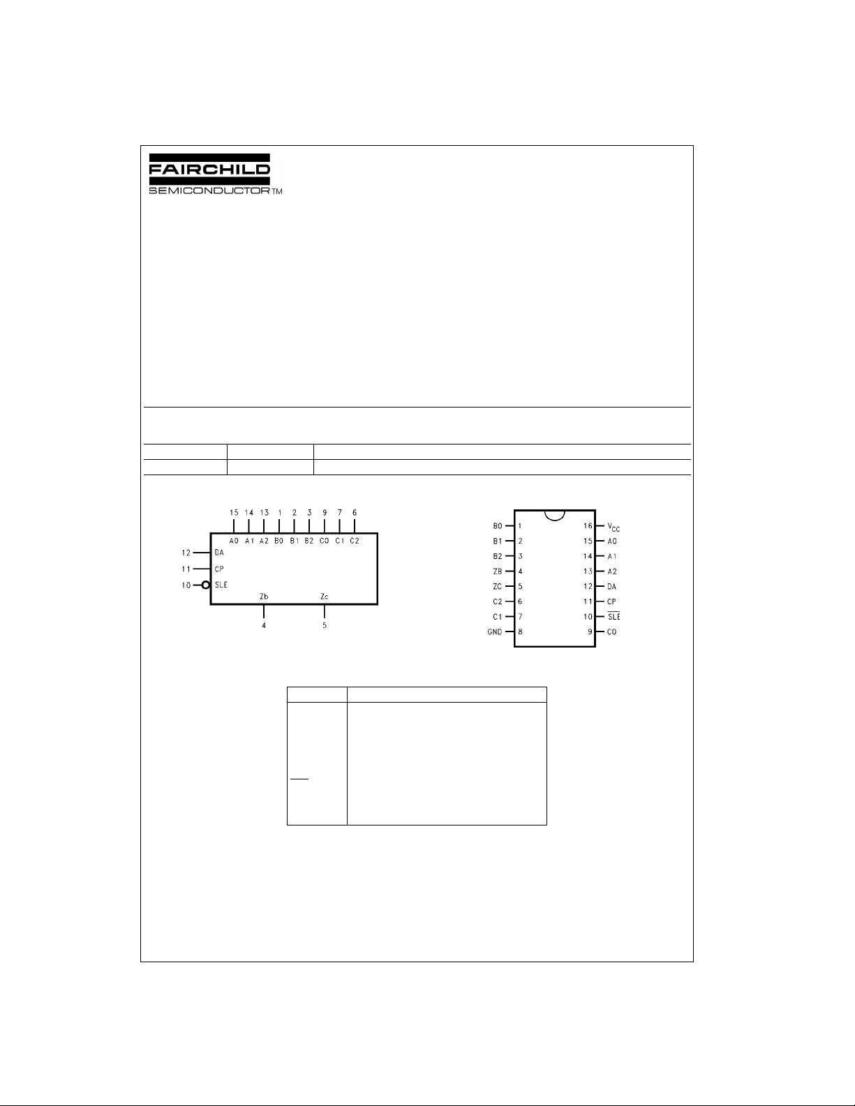
Logic Symbol
VCC = Pin 16
GND = Pin 8
Connection Diagram
Pin Descriptions
Pin Names Description
A0–A2 Write Address Inputs
DA Data Input
B0–B2 B Read Address Inputs
C0–C2 C Read Address Inputs
CP Clock Pulse Input (Active Rising Edge)
SLE
ZB B Output
ZC C Output
Slave Enable Input (Active LOW)
© 2000 Fairchild Semiconductor Corporation DS010202 www.fairchildsemi.com

Functional Description
The DM93L38 8-b it multiple port register can be consi dered a 1-bit slice of eight high speed working registers.
Data can be written in to any on e and r ead fro m any two of
DM93L38
the eight locations sim ultaneously. Master/slave operation
eliminates all race problems associated with simultaneous
read/write activity from the same location. When t he clock
input (CP) is LOW data applied to the d ata input line (D
enters the selected master. This selection is accomplished
by coding the three write input select lin es (A0–A 2) appropriately. Data is stored synchronously with the ri sing edge
of the clock pulse.
The information for each of the two slaved (output) latches
is selected by two sets o f read a ddress i npu ts (B0–B2 and
C0–C2). The information enters the slave while the clock is
HIGH and is stored while the clock is LOW. If Slave Enable
is LOW (SLE
), the slave latches are co ntinu ously en able d.
The signals are availab le on the output pins (Z
The input bit selection and the two output bit selections can
be accomplished independently or simultaneously. The
data flows into the device, is demultiplexed according to
the state of the write addre ss lines and is clocke d into the
selected latch. The eight latche s function as masters and
)
store the input data. The two ou tpu t l atch es ar e slave s and
A
hold the data during the read operatio n. The sta te of each
slave is determined by the sta te of the master sele cted by
its associated set of read address inputs.
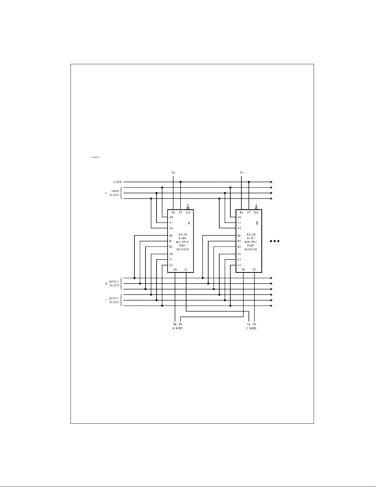
The method of parallel expansion is shown in Figure 1.
One DM93L38 is n eeded for each bit o f the req uired wo rd
length. The read an d w r ite inp ut l in es sh ou l d be con nec ted
in common on all of the devices. This register configuration
provides two words of n-bits each at one time, where n
devices are connected in parallel.
and ZC).
B
FIGURE 1. Parallel Expansion
www.fairchildsemi.com 2
 Loading...