

Fairchild Semiconductor DM93L14N, DM93L14CW Datasheet
© 1999 Fairchild Semiconductor Corporation DS009612 www.fairchildsemi.com
June 1989
Revised November 1999
DM93L14 Quad Latch
DM93L14
Quad Latch
General Description
The DM93L14 is a mul tifunctional 4-bit latch designed for
general purpose s torage appl ications in high spe ed digital
systems. All outputs have active pull-up circuitry to provide
high capacitance drive and to provide low im pedance in
both logic states for good noise immunity.
Features
■ Can be used as single input D latches or set/reset
latches
■ Active low enable gate input
■ Overriding master reset
Ordering Code:
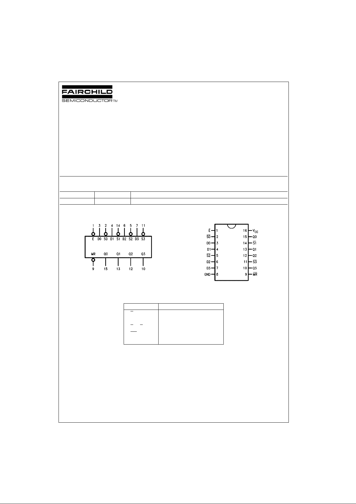
Logic Symbol
VCC = Pin 16
GND = Pin 8
Connection Diagram
Pin Descriptions
Order Number Package Number Package Description
DM93L14N N14A 14-Lead Plastic Dual-In-Line Package (PDIP), JEDEC MS-001, 0.300 Wide
Pin Names Description
E
Enable Input (Active LOW)
D0 − D3 Data Inputs
S
0 − S3 Set Inputs (Active LOW)
MR
Master Reset Input (Active LOW)
Q0 − Q3 Latch Outputs
www.fairchildsemi.com 2
DM93L14
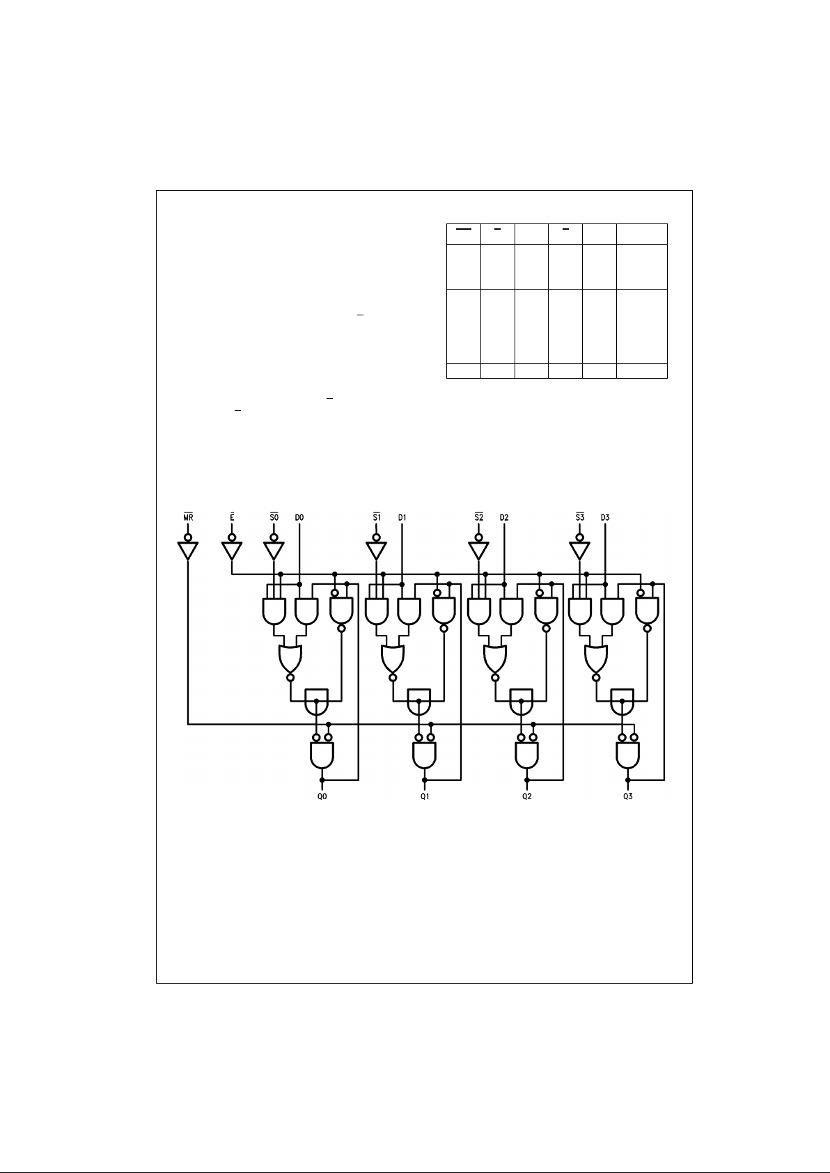
Functional Description
The DM93L14 consists of four latches with a common
active LOW Enable input and active LOW Master Reset
input. When the E nable goes HIGH, data present i n the
latches is stored a nd the state of the latch is no longer
affected by the S
n
and Dn inputs. the Master Reset when
activated overrides all other input conditions forcing all
latch outputs LOW. Each of the four latches can be operated in one of two modes:
D-TYPE LATCH—For D-type operation the S
input of a
latch is held LOW. While the common Enable is active the
latch output follo ws the D input. Infor mation pr esent at th e
latch output is stored in the latch when the Enable go es
HIGH.
SET/RESET LATCH—During set/reset op eration when th e
common Enable is LOW a latch is reset by a LOW on the D
input, and can be set by a LOW on the S
input if the D input
is HIGH. If both S
and D inputs are LOW, the D input will
dominate and the latch will be reset. When the Enable
goes HIGH, the la tch rema ins in t he last st ate prior to disablement. The two modes of la tch operat ion are shown in
the Truth Table.
Tr uth Table
H = HIGH Voltage Level
L = LOW Voltage Level
X = Immaterial
Q
n−1
= Previous Output St ate
Q
n
= Present Output State
Logic Diagram
MR E
D
S
Q
n
Operation
HLLLLD Mode
HLHLL
HHXXQ
n-1
HLLLLR/S Mode
HLHLH
HLLHL
HLHHQ
n-1
HHXXQ
n-1
L X X X L RESET
 Loading...