

Fairchild Semiconductor DM9370N Datasheet
© 2000 Fairchild Semiconductor Corporation DS009797 www.fairchildsemi.com
October 1988
Revised March 2000
DM9370 7-Segment Decoder/Driver/Latch with Open-Collector Outputs
DM9370
7-Segment Decoder/Driver/Latch
with Open-Collector Outputs
General Description
The DM9370 is a 7-se gment decoder driver incorporating
input latches and outp ut circuits to dire ctly drive i ncandescent displays. It c an also b e used to driv e common a node
LED displays in either a multiplexed mode or directly with
the aid of external current limiting resistors.
Ordering Code:
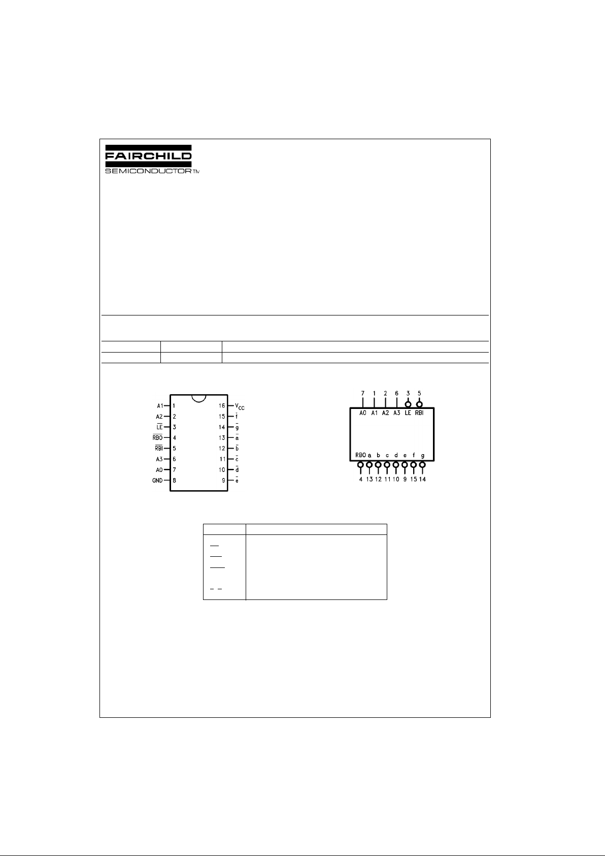
Connection Diagram Logic Symbol
VCC = Pin 16
GND = Pin 8
Pin Descriptions
Order Number Package Number Package Description
DM9370 N16E 16-Lead Plastic Dual-In-Line Package (PDIP), JEDEC MS-001, 0.300 Wide
Pin Names Description
A0–A3 Address Inputs
LE
Latch Enable Input (Active LOW)
RBI
Ripple Blanking Input (Active LOW)
RBO
Ripple Blanking as Output (Active LOW)
as Input (Active LOW)
a
–g Segment Outputs (Active LOW)
www.fairchildsemi.com 2
DM9370
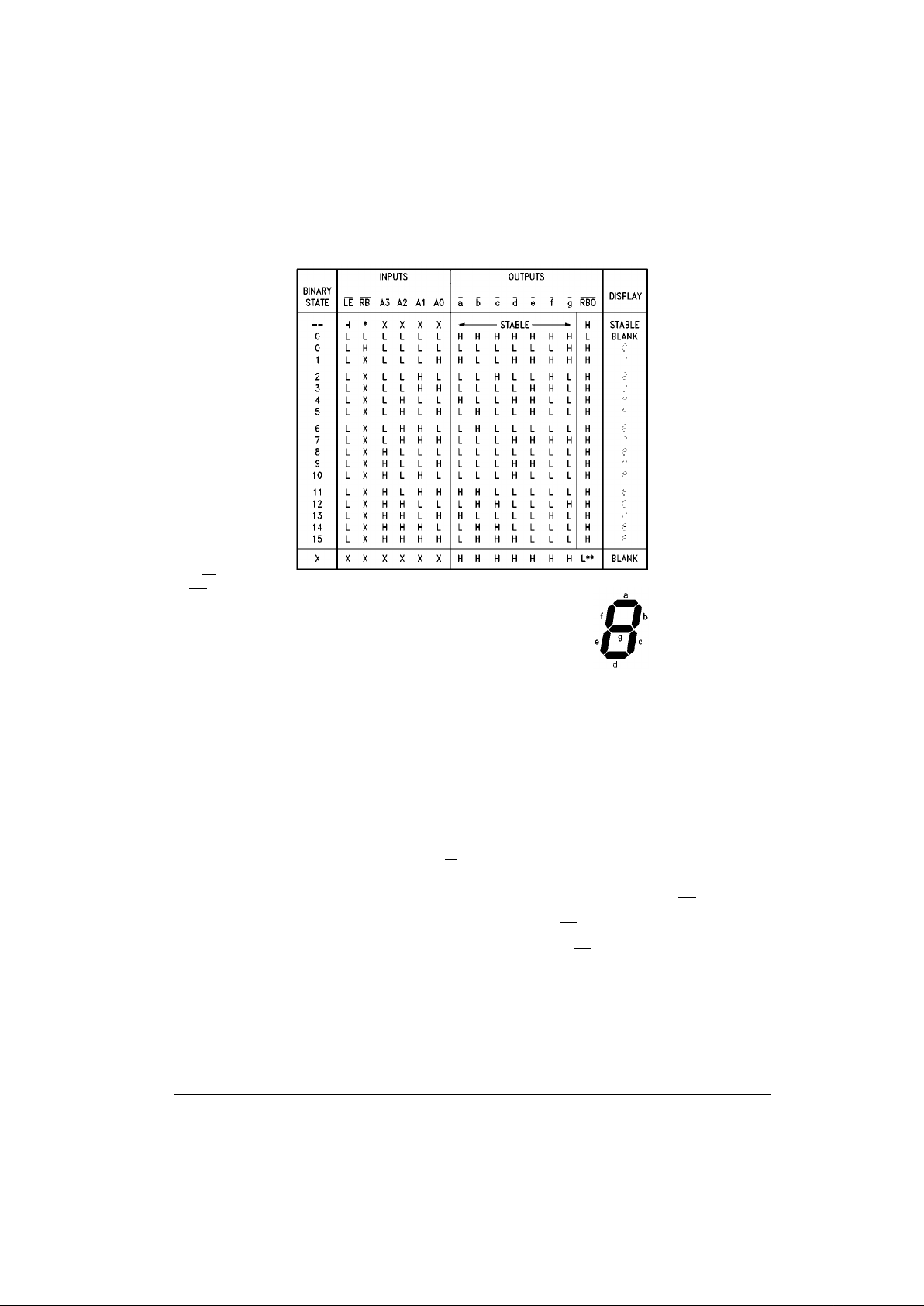
Truth Table
*The RBI will blank the display on ly if b inary zero is stored in the lat c hes.
**RBO
used as an input over drives all other input con dit ions.
H = HIGH Voltage Level
L = LOW Voltage Level
X = Immaterial
Functional Description
The DM9370 has active LOW outputs capable of sinking in
excess of 25 mA which allows it to drive a wide variety of 7segment incandescent displays directly. It may also be
used to drive common anode LED displays, multiplex ed or
directly with the aid of suitable current limiting resistors.
This device accepts a 4-bit bina ry code and p roduces ou tput drive to the appropriate segments of the 7-segment display. It has a hexadecimal decode forma t which produces
numeric codes “0” through “9” and alpha codes “A” through
“F” using upper and lower case fonts.
Latches on the fo ur dat a input s are c ontr olled b y an ac tive
LOW latch enable LE
. When the LE is LOW, the state of
the outputs is determin ed by the input data. W hen the LE
goes HIGH, the last data present at the inputs is stored in
the latches and the outputs remain stable. The LE
pulse
width necessary to accept and store data is typically 30 ns
which allows data to be strobed into the DM9370 at normal
TTL speeds. This fea ture means that data can be routed
directly from high s peed counters and freque ncy dividers
into the display without slowing down the system clock or
providing intermediate data storage.
The latch/decoder combinatio n is a simple system which
drives incandescent displ ays with multiplexed data inputs
from MOS time clocks, DVMs, calc ulator chips, etc. Data
inputs are multiplexed while the displays are in static mode.
This lowers component and ins ertion costs since several
circuits—seven diodes per display, strobe drivers, a separate display voltage source, and clock failure detect cir-
cuits—traditionally found in incandescent multiplexed
display systems are elim inated. It also al lows low strob ing
rates to be used without display flicker.
Another DM9370 feature is the reduced loading on the
data inputs when the Latch Enable is HIGH (only 10 µA
typ). This allows many DM9370s to be driven from a MOS
device in multiplex mod e without the need for drivers on
the data lines. The DM9370 also provides automatic blanking of the leading and/or trailing-edge zeroes in a multidigit
decimal number, resulting in an easily readable decimal
display conforming to no rmal writing p ractice. In an 8- digit
mixed integer fraction decimal representation, using the
automatic blanking capability, 0060.0300 would be displayed as 60.03. Leading-edge zero suppression is
obtained by connecting the Ripple Blan king Output (RBO
)
of a decoder to t he Rippl e Blan king Input (RBI
) of the next
lower stage device. The most significant decoder stage
should have the RBI
input grounded; an d since suppression of the least significa nt integer ze ro in a n umber is not
usually desired, the RBI
input of this decoder stage sho uld
be left open. A sim ila r pro c ed ur e f or the fractional part of a
display will provide automatic suppression of trailing-edge
zeroes. The RBO
terminal of the decoder can be OR-tied
with a modulating signal via an iso lating buffer to achieve
pulse duration intens ity modulation. A suitable signal can
be generated for this pur pose by forming a variable frequency multivibrator with a cross coupled pair of TTL or
DTL gates.
 Loading...