

Fairchild Semiconductor DM9328N Datasheet
October 1988
Revised February 2000
DM9328
Dual 8-Bit Shift Register
General Description
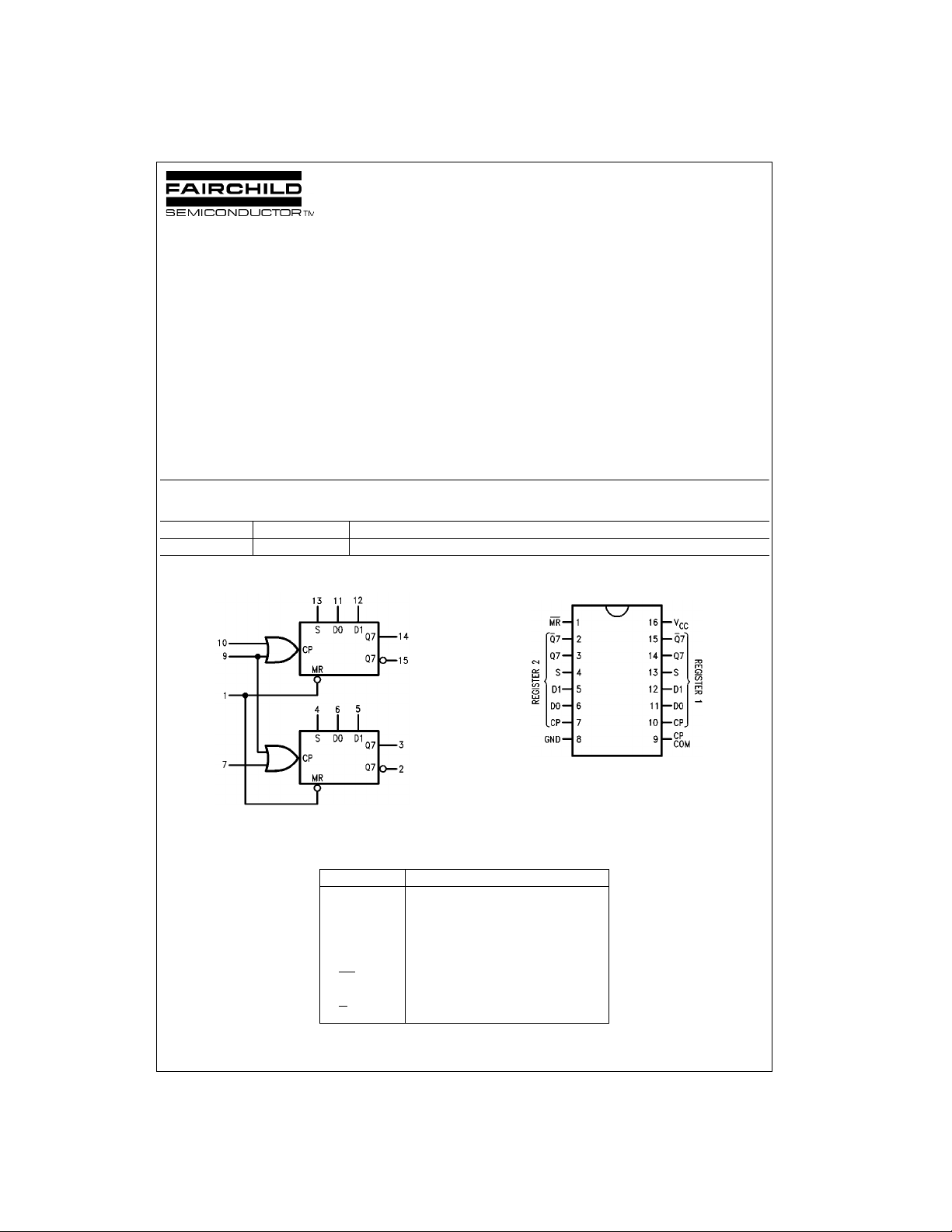
The DM9328 is a high speed serial storage element providing 16 bits of storage in the for m o f tw o 8- bit r egi s ter s. T he
multifunctional capability of this device is provided by several features: 1) additional gating is provided at the input to
both shift registers so that the inpu t is easily multiplexed
between two sources; 2) the cl ock of each re gister ma y be
provided separately or to gether; 3) both the tru e and complementary outputs are provided from each 8-bit register,
and both registers may be master cl eared from a comm on
input.
Ordering Code:
Order Number Package Number Package Description
DM9328N N16E 16-Lead Plastic Dual-In-Line Package (PDIP), JEDEC MS-001, 0.300 Wide
DM9328 Dual 8-Bit Shift Register
Logic Symbol
VCC = Pin 16
GND = Pin 8
Pin Descriptions
Connection Diagram
Pin Names Description
S Data Select Input
D0, D1 Data Inputs
CP Clock Pulse Input (Active HIGH)
Common (Pin 9)
Separate (Pins 7 and 10)
MR
Q7 Last Stage Output
7 Complementary Output
Q
Master Reset Input (Active LOW)
© 2000 Fairchild Semiconductor Corporation DS009793 www.fairchildsemi.com
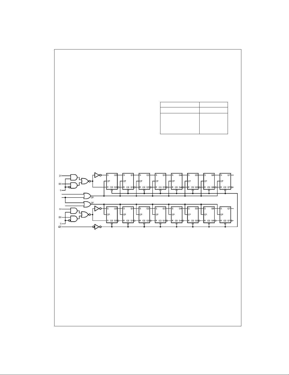
Functional Description
The two 8-bit shift registe rs have a common clock input
(pin 9) and separate clock inputs (pins 10 and 7). The
DM9328
clocking of each register is controlled by the OR function of
the separate and the commo n clock in put. Each registe r is
composed of eight clocked RS master/slave flip-flops and a
number of gates . The clock OR g ate dr ives the eig ht cl ock
inputs of the flip-flops in parallel. When the two clock inputs
(the separate and the co mmon) to the OR gate are LOW,
the slave latches are ste ad y, but data can enter the maste r
latches via the R and S input. During the first LOW-toHIGH transition of either, or both simultaneously, of the two
clock inputs, the data inputs (R and S) are inhibited so that
a later change in input data will not affect the maste r; then
the now trapped informa tion in the master is transferred to
the slave. When the transfer is complete, both the m aster
and the slave a re steady as long as eith er or both clock
inputs remain HIGH. During the HIGH- to- LOW transition of
the last remaining HIG H clock inp ut, the tr ansfer path fro m
master to slave is inhibited first, leaving the slave steady in
its present state. The data inputs (R and S) are enabled so
that new data can enter the master. Either of the clock
inputs can be use d as clock inhibit inputs by applying a
logic HIGH signal. Each 8-bit shift register h as a 2-input
Logic Diagram
multiplexer in front of the serial dat a input. The two data
inputs D0 and D1 are controlled by the data select input (S)
following the Boolean expression:
Serial data in: S
An asynchronous master reset is provided which, when
activated by a LOW logic level, will clear all 16 stages independently of any other input signal.
= SD0 + SD1
D
Shift Select Table
INPUTS OUTPUT
SD0D1 Q7 (t
LL X L
LH X H
HX L L
H = HIGH Voltage Level
L = LOW Voltage Level
X = Immaterial
n + 8 = indicates state after eight clock pulse
HX H H
n + 8
)
www.fairchildsemi.com 2
 Loading...