

Fairchild Semiconductor DM81LS97AN, DM81LS95AWM, DM81LS95AN Datasheet
DM81LS95A • DM81LS96A • DM81LS97A
3-STATE Octal Buffer
DM81LS95A • DM81LS96A • DM81LS97A 3-STATE Octal Buffer
September 1991
Revised May 1999
General Description
These devices provide eight, two-input buffers in each
package. All employ low-po wer-Schottky TTL technology.
One of the two in puts to each buffer is used as a control
line to gate the output into the high-im pedan ce state, whi le
the other input passes the data through the buffer. The
DM81LS95A and DM81LS97A present true data at the outputs, while the DM81LS96A is inverting. On the
DM81LS95A and DM81LS96A versions, all eigh t 3-STATE
enable lines are common, w ith access through a 2-input
NOR gate. On the DM81LS97A vers ion, four buffers are
enabled from one commo n line, and the other four buffers
are enabled form anoth er common line. In all cases the
outputs are placed in the 3-STATE condition by applying a
high logic level to the enable pins.
Features
■ Typical power dissipation
DM81LS95A, DM81LS97A 80 mW
DM81LS96A 65 mW
■ Typical propagation delay
DM81LS95A, DM81LS97A 15 ns
DM81LS96A 10 ns
■ Low power-Schottky, 3-STAT E technology
Ordering Code:
Order Number Package Number Package Description
DM81LS95AWM M20B 20-Lead Small Outline Integrated Circuit (SOIC), JEDEC MS-013, 0.300 Wide
DM81LS95AN N20A 20-Lead Plastic Dual-In-Line Package (PDIP), JEDEC MS-001, 0.300 Wide
DM81LS96AWM M20B 20-Lead Small Outline Integrated Circuit (SOIC), JEDEC MS-013, 0.300 Wide
DM81LS96AN N20A 20-Lead Plastic Dual-In-Line Package (PDIP), JEDEC MS-001, 0.300 Wide
DM81LS97AN N20A 20-Lead Plastic Dual-In-Line Package (PDIP), JEDEC MS-001, 0.300 Wide
Devices also availab le in Tape and Reel. Specify by appending th e s uffix let t er “X” to the ordering cod e.
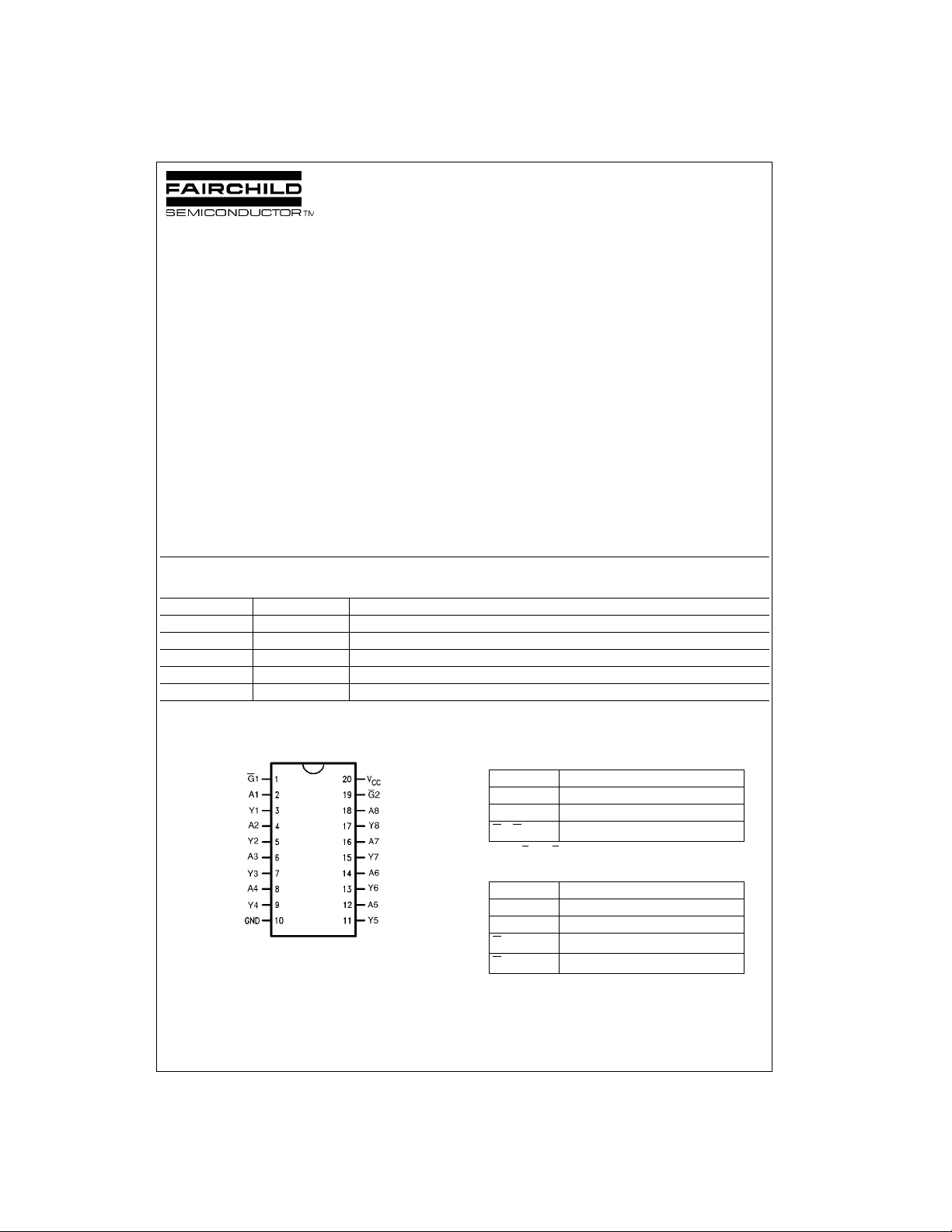
Connection Diagram Pin Descriptions
DM81LS95A and DM92 LS96A
Pin Names Descriptions
A1–A8 Inputs
Y1–Y8 Outputs
1–G2
G
Note 1: Both G1 and G2 must be LOW for outpu ts t o be enabled.
Pin Names Descriptions
A1–A8 Inputs
Y1–Y8 Outputs
1
G
2
G
Active LOW Output Enables (Note 1)
DM81LS97A
Active LOW Output Enable (Y1–Y4)
Active LOW Output Enable (Y5–Y8)
© 1999 Fairchild Semiconductor Corporation DS006435 www.fairchildsemi.com

Logic Symbols
DM81LS95A
Truth Tables
1G2A Y
G
H X X Hi-Z
X H X Hi-Z
LLHH
LLLL
DM81LS95A
Inputs Output
DM81LS95A • DM81LS96A • DM81LS97A
DM81LS96A
DM81LS97A
DM81LS96A
Inputs Output
1G2A Y
G
H X X Hi-Z
X H X Hi-Z
LLH L
LLL H
DM81LS97A
Inputs Output
1 A1–A4 Y1–Y4
G
H X Hi-Z
LHH
LLL
2 A5–A6 Y5–Y8
G
H X Hi-Z
LHH
LLL
www.fairchildsemi.com 2
Absolute Maximum Ratings(Note 2)
Supply Voltage 7V
Input Voltage 7V
Operating Free Air Temperature Range 0°C to +70°C
Storage Temperature Range −65°C to +150°C
Note 2: The Absolute Maximum Ratings are those values beyond which
the safety of the device cannot be guaranteed. The device should not be
operated at these limits. The parametric values defined in the Electrical
Characteristics tables are not guaranteed at the absolute maximum ratings.
The Recommende d Operating Con ditions table will def ine the conditions
for actual device operation.
Recommended Operating Conditions
Symbol Parameter Min Nom Max Units
V
CC
V
IH
V
IL
I
OH
I
OL
T
A
Supply Voltage 4.75 5 5.25 V
HIGH Level Input Voltage 2 V
LOW Level In put Voltage 0.8 V
HIGH Level Output Current −5.2 mA
LOW Level Ou tput Current 24 mA
Free Air Operating Temperature 0 70 °C
DM81LS95A • DM81LS96A • DM81LS97A
3 www.fairchildsemi.com
 Loading...