

Fairchild Semiconductor DM74S74N, DM74S74MX, DM74S74M, DM74S74CW Datasheet
© 2000 Fairchild Semiconductor Corporation DS006457 www.fairchildsemi.com
August 1986
Revised April 2000
DM74S74 Dual Positive-Edge-Triggered D Flip-Flops with Preset, Clear, and Complementary Outputs
DM74S74
Dual Positive-Edge-Triggered D Flip-Flops
with Preset, Clear, and Complementary Outputs
General Description
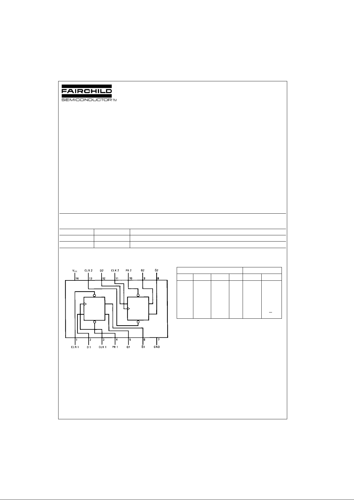
This device contains two independent positive-edge-triggered D flip-flops with c omplementary outputs. The information on the D inp ut is accepted by the f lip-flops on the
positive going edge of the clock pulse. The triggering
occurs at a voltage level and is not directly relat ed to the
transition time of the rising edg e of the clock. The data on
the D input may be changed while the clock is LOW or
HIGH without affecting the outpu ts as long as setup and
hold times are not violated. A low logic level on the preset
or clear inputs will set or reset the outputs regardless of the
logic levels of the other inputs.
Ordering Code:
Devices also availab le in Tape and Reel. Specify by appending th e s uffix let t er “X” to the ordering code.
Connection Diagram Function Table
H = HIGH Logic Level
X = Either LOW or HIGH Logic Level
L = LOW Logic Level
↑ = Positive-going Transition
* = This configuration is nonstable ; th at is , it will not persist w hen either the
preset and/or clear in puts return to its inactive (H I GH ) level.
Q
0
= The output logic level of Q before the indicated input conditions were
established.
Order Number Package Number Package Description
DM74S74M M14A 14-Lead Small Outline Integrated Circuit (SOIC), JEDEC MS-120, 0.150 Narrow
DM74S74N N14A 14-Lead Plastic Dual-In-Line Package (PDIP), JEDEC MS-001, 0.300 Wide
Inputs Outputs
PR CLR CLK D Q Q
LHXXH L
HL XXL H
L L X X H* H*
HH ↑ HH L
HH ↑ LL H
HH LXQ
0
Q
0
www.fairchildsemi.com 2
DM74S74
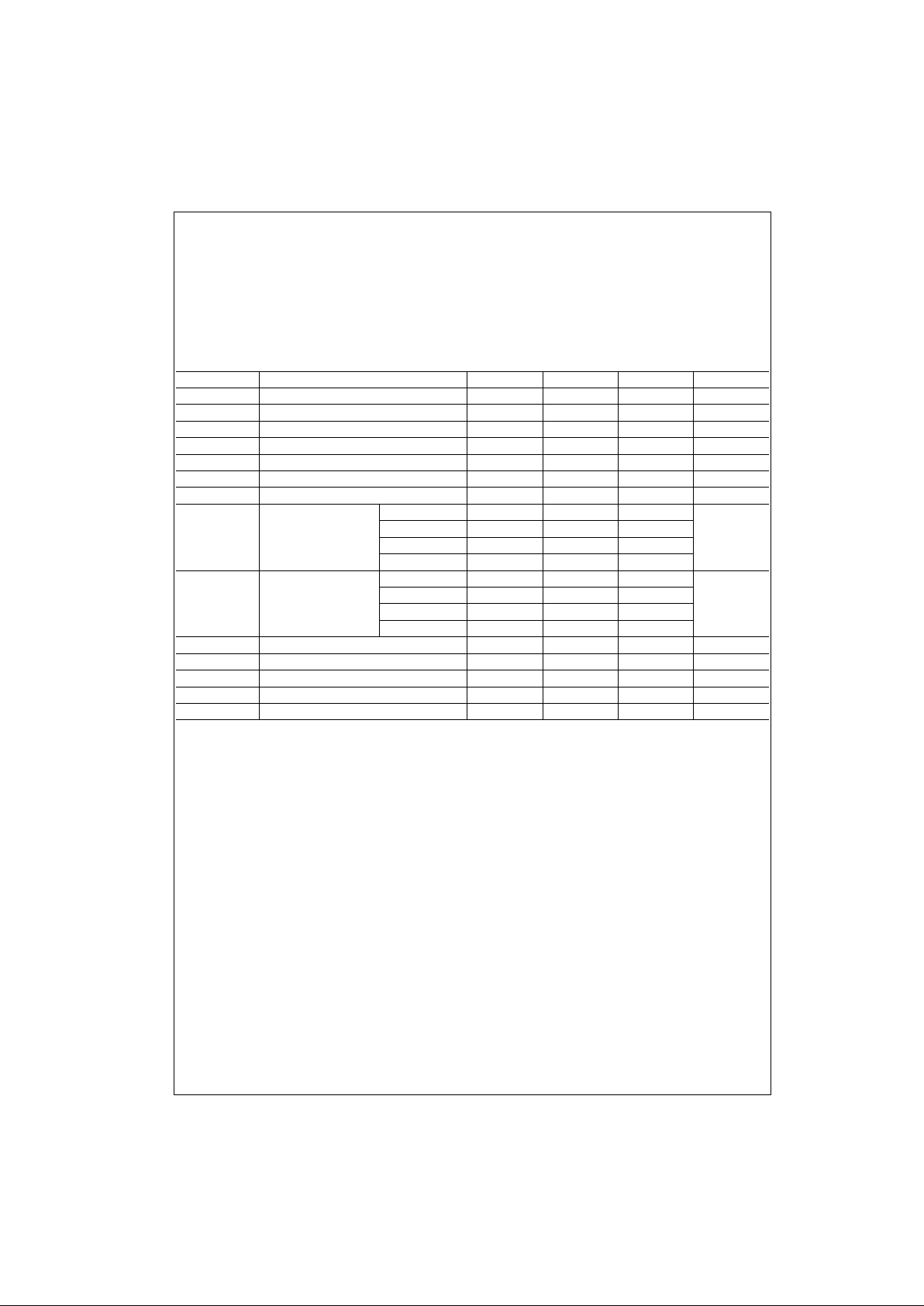
Absolute Maximum Ratings(Note 1)
Note 1: The “Absolute Maximum Ratings” are those values beyon d which
the safety of the dev ice cannot be guaranteed. T he device sh ould not be
operated at these limit s. The parametric values defin ed in the Electrical
Characteristics tables are not guaranteed at the absolute maximum ratings.
The “Recomme nded O peratin g Cond itions ” table will defin e the condition s
for actual device operation.
Recommended Operating Conditions
Note 2: CL = 15 pF, RL = 280Ω, TA = 25°C and VCC = 5V.
Note 3: C
L
= 50 pF, RL = 280Ω, TA = 25°C and VCC = 5V.
Note 4: The symbol (↑) indicates the rising edge at the clock puls e is us ed for reference.
Supply Voltage 7V
Input Voltage 5.5V
Operating Free Air Temperature Range 0°C to +70°C
Storage Temperature Range −65°C to +150°C
Symbol Parameter Min Nom Max Units
V
CC
Supply Voltage 4.75 5 5.25 V
V
IH
HIGH Level Input Voltage 2 V
V
IL
LOW Level Input Voltage 0.8 V
I
OH
HIGH Level Output Current −1mA
I
OL
LOW Level Output Current 20 mA
f
CLK
Clock Frequency (Note 2) 0 110 75 MHz
f
CLK
Clock Frequency (Note 3) 0 95 65 MHz
t
W
Pulse Width Clock HIGH 6
(Note 2) Clock LOW 7.3
ns
Clear LOW 7
Preset LOW 7
t
W
Pulse Width Clock HIGH 8
(Note 3) Clock LOW 9
ns
Clear LOW 9
Preset LOW 9
t
SU
Setup Time (Note 2)(Note 4) 3↑ ns
t
SU
Setup Time (Note 3)(Note 4) 3↑ ns
t
H
Input Hold Time (Note 2)(Note 4) 2↑ ns
t
H
Input Hold Time (Note 3)(Note 4) 2↑ ns
T
A
Free Air Operating Temperature 0 70 °C
 Loading...