

Fairchild Semiconductor DM74S51N Datasheet
August 1986
Revised April 2000
DM74S51
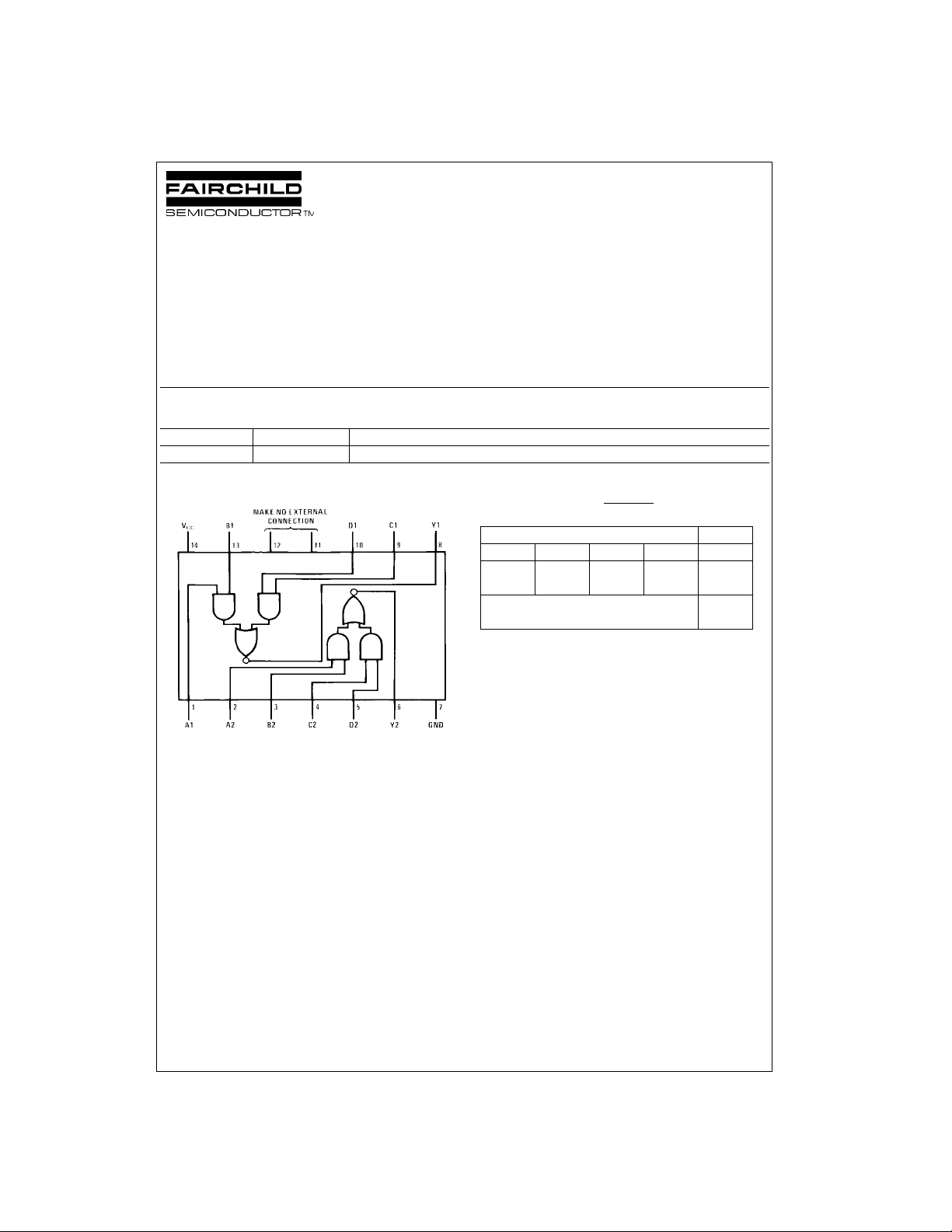
Dual 2-Wide 2-Input AND-OR-INVERT Gate
General Description
This device contains two independent combinations of
gates each of which perform s the logic AND-OR-INVERT
function.
Ordering Code:
Order Number Package Number Package Description
DM74S51N N14A 14-Lead Plastic Dual-In-Line Package (PDIP), JEDEC MS-001, 0.300 Wide
Connection Diagram Function Table
Y = AB + CD
Inputs Output
ABCDY
HHXXL
XXHHL
All other H
H = HIGH Logic Level
L = LOW Logic Level
X = Either LOW or HIGH Logic Level
combinations
DM74S51 Dual 2-Wide 2-Input AND-OR-INVERT Gate
© 2000 Fairchild Semiconductor Corporation DS006454 www.fairchildsemi.com
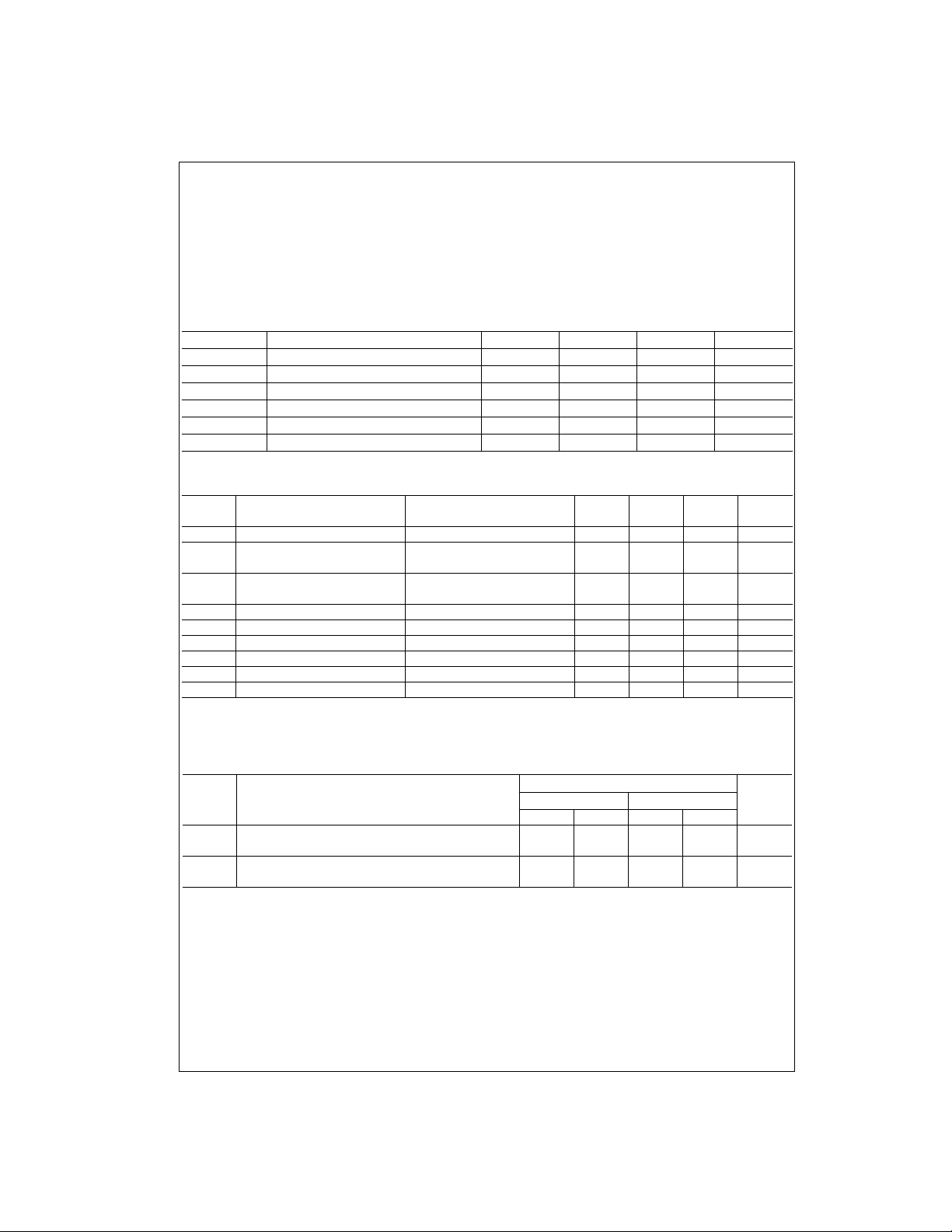
Absolute Maximum Ratings(Note 1)
Supply Voltage 7V
Input Voltage 5.5V
DM74S51
Operating Free Air Temperature Range 0°C to +70°C
Storage Temperature Range −65°C to +150°C
Note 1: The “Absolute Maximum Ratin gs” are those v alues beyon d which
the safety of the dev ice cannot be guaranteed. T he device sh ould not be
operated at these limits. The parametric values defined in the Electrical
Characteristics tables are not guaranteed at the absolute maximum ratings.
The “Recommend ed O peratin g Cond itions” t able w ill defin e the c ondit ions
for actual device operation.
Recommended Operating Conditions
Symbol Parameter Min Nom Max Units
V
CC
V
IH
V
IL
I
OH
I
OL
T
A
Supply Voltage 4.75 5 5.25 V
HIGH Level Input Voltage 2 V
LOW Level Input Voltage 0.8 V
HIGH Level Output Current −1mA
LOW Level Output Current 20 mA
Free Air Operating Temperature 0 70 °C
Electrical Characteristics
over recommended operating free air temperature (unless otherwise noted)
Symbol Parameter Conditions Min
V
I
V
OH
V
OL
I
I
I
IH
I
IL
I
OS
I
CCH
I
CCL
Note 2: All typicals are at VCC = 5V, TA = 25°C.
Note 3: Not more than one output should be shorted at a time, and the duration should not exceed one second.
Input Clamp Voltage VCC = Min, II = −18 mA −1.2 V
HIGH Level VCC = Min, IOH = Max
Output Voltage VIL = Max
LOW Level VCC = Min, IOL = Max
Output Voltage VIH = Min
Input Current @ Max Input Voltage VCC = Max, VI = 5.5V 1 mA
HIGH Level Input Current VCC = Max, VI = 2.7V 50 µA
LOW Level Input Current VCC = Max, VI = 0.5V −2mA
Short Circuit Output Current VCC = Max (Note 3) −40 −100 mA
Supply Current with Outputs HIGH VCC = Max 8.2 17.8 mA
Supply Current with Outputs LOW VCC = Max 14 22 mA
2.7 3.4 V
Typ
(Note 2)
Max Units
0.5 V
Switching Characteristics
at VCC = 5V and TA = 25°C
Symbol Parameter
t
PLH
t
PHL
www.fairchildsemi.com 2
Propagation Delay Time
LOW-to-HIGH Level Output
Propagation Delay Time
HIGH-to-LOW Level Output
RL = 280Ω
CL = 15 pF CL = 50 pF
Min Max Min Max
25.53 8ns
25.53 8ns
Units
 Loading...