

Fairchild Semiconductor DM74S374WM, DM74S374N, DM74S373WM, DM74S373N Datasheet
DM74S373 • DM74S374
3-STATE Octal D-Type Transparent Latches
and Edge-Triggered Flip-Flops
DM74S373 • DM74S374 3-STATE Octal D-Type Transparent Latches and Edge-Triggered Flip-Flops
August 1986
Revised May 2000
General Description
These 8-bit regist ers feature totem-pole 3-STATE outputs
designed specifically fo r driving highly-capacitive or relatively low-impedance loa ds. Th e high-impedance state and
increased high-logic-level drive provide these registers with
the capability of being connected directly to and driving the
bus lines in a bu s-or ga nized system without need for interface or pull-up components. They are particularly attractive
for implementing buffer registers, I/O ports, bidirectional
bus drivers, and working registers.
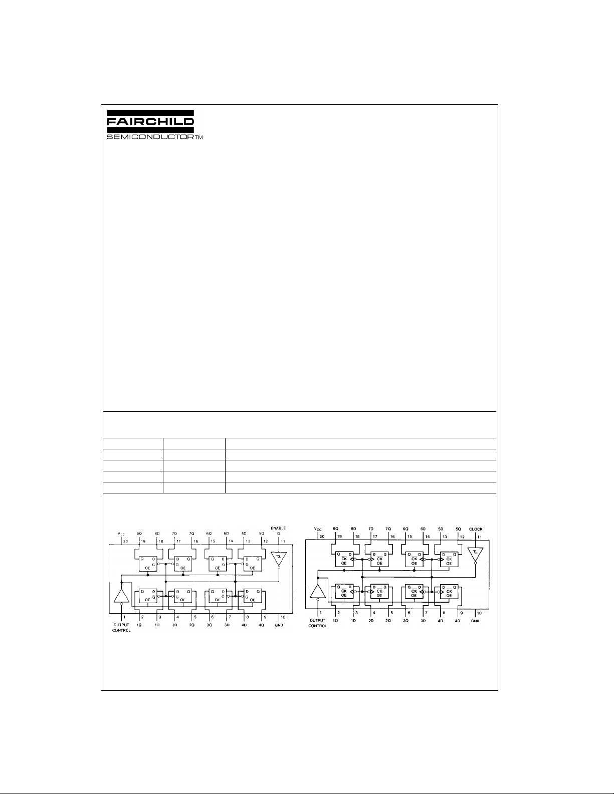
The eight latches of the DM 74 S373 are tran spa ren t D -ty pe
latches meaning that while the en able (G) is HIGH the Q
outputs will follow the da ta (D) inputs. When the ena ble is
taken LOW the output will be latched at the level of the
data that was set up.
The eight flip-flops of the DM74S374 are edge-triggered Dtype flip-flops. On the positive tr ansit ion of the clock , the Q
outputs will be set to the logic states that were set up at the
D inputs.
Schmitt-trigger buffered inputs at the enable/clock lines
simplify system design as ac and dc noise rejection is
improved by typically 400 mV due to the input hysteresis. A
buffered output control input can be used to place the eight
outputs in either a norm al logic state (HIG H or LOW logic
levels) or a high -impedance state. In the high-impedance
state the outputs neither load nor drive the bus lines significantly.
The output control does no t affect the intern al operation of
the latches or flip-flops. That is, the old data can be
retained or new data can be entered even while the outputs
are OFF.
Features
■ Choice of 8 latches or 8 D-type flip-flops in a single
package
■ 3-STATE bus-driving outputs
■ Full parallel-access for loading
■ Buffered control inputs
■ P-N-P input reduce D-C loading on data lines
Ordering Code:
Order Number Package Number Package Description
DM74S373WM M20B 20-Lead Small Outline Integrated Circuit (SOIC), JEDEC MS-013, 0.300 Wide
DM74S373N N20A 20-Lead Plastic Dual-In-Line Package (PDIP), JEDEC MS-001, 0.300 Wide
DM74S374WM M20B 20-Lead Small Outline Integrated Circuit (SOIC), JEDEC MS-013, 0.300 Wide
DM74S374N N20A 20-Lead Plastic Dual-In-Line Package (PDIP), JEDEC MS-001, 0.300 Wide
Devices also availab le in Tape and Reel. Specify by appending the suffix letter “X” to the o rdering code.
Connection Diagrams
DM74S373N
© 2000 Fairchild Semiconductor Corporation DS006486 www.fairchildsemi.com
DM74S374N
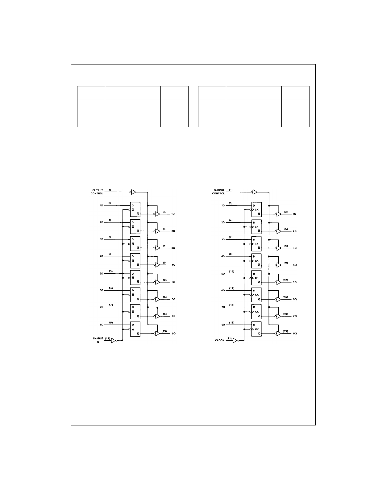
Truth Tables
DM74S373
Output Enable D Output
Control G
LHHH
LHLL
LLXQ
HXXZ
H = HIGH Level (Steady State)
L = LOW Level (Stea dy State)
DM74S373 • DM74S374
X = Don’t Care
Z = High Impedance State
↑ = Transition from LOW-to-HIGH lev el,
= T he level of the output before steady-st ate input conditions were
Q
0
established.
Logic Diagrams
DM74S374
Output Clock D Output
Control
L ↑ HH
L ↑ LL
0
LLXQ
0
HXXZ
74S373
Transparent Latches
Positive-Edge-Triggered Flip-Flops
74S374
www.fairchildsemi.com 2
Absolute Maximum Ratings(Note 1)
Supply Voltage 7V
Input Voltage 5.5V
Operating Free Air Temperature Range 0°C to +70°C
Storage Temperature Range −65°C to +150°C
Note 1: The “Absolute Maximum Ratings” are those value s beyond which
the safety of the d evice cannot b e guaranteed . The device sh ould not be
operated at these limit s. The parametric values defi ned in the Electrical
Characteristics tables ar e not guaranteed at t he absolute maximum ratings.
The “Recomm ended O peratin g Cond itions ” table will defin e the condition s
for actual device operation.
DM74S373 Recommended Operating Conditions
Symbol Parameter Min Nom Max Units
V
CC
V
IH
V
IL
I
OH
I
OL
t
W
t
W
t
SU
t
H
T
A
Note 2: CL = 15 pF, RL = 280Ω, TA = 25°C and VCC = 5V.
Note 3: C
Note 4: The symbol (↓) indicates the falling edge of the clock pulse is used for reference.
Note 5: T
Supply Voltage 4.75 5 5.25 V
HIGH Level Input Voltage 2 V
LOW Level Input Voltage 0.8 V
HIGH Level Output Current −6.5 mA
LOW Level Output Current 20 mA
Pulse Width (Note 2) Enable HIGH 6
Enable LOW 7.3
Pulse Width (Note 3) Enable HIGH 15 ns
Enable LOW 15 ns
Data Setup Time (Note 4)(Note 5) 0↓ ns
Data Hold Time (Note 4)(Note 5) 10↓ ns
Free Air Operating Temperature 0 70 °C
= 50 pF and RL = 280Ω, TA = 25°C and VCC = 5V.
L
= 25°C and VCC = 5V.
A
DM74S373 • DM74S374
ns
DM74S373 Electrical Characteristics
over recommended operating free air temperature (unless otherwise noted)
Symbol Parameter Conditions Min
V
I
V
OH
V
OL
I
I
I
IH
I
IL
I
OZH
I
OZL
I
OS
I
CC
Note 6: All typi c als are at VCC = 5V, TA = 25°C.
Note 7: Not more than one output sh ould be shorted at a time, and the duration should not exceed one s ec ond.
Input Clamp Voltage VCC = Min, II = −18 mA −1.2 V
HIGH Level VCC = Min, IOH = Max
Output Voltage VIL = Max, VIH = Min
LOW Level VCC = Min, IOL = Max
Output Voltage V
= Min, VIL = Max
IH
Input Current @ Max Input Voltage VCC = Max, VI = 5.5V 1 mA
HIGH Level Input Current VCC = Max, VI = 2.7V 50 µA
LOW Level Input Current VCC = Max, VI = 0.5V −250 µA
Off-State Output Current with VCC = Max, VO = 2.4V
HIGH Level Output Voltage Applied VIH = Min, VIL = Max
Off-State Output Current with VCC = Max, VO = 0.5V
LOW Level Output Voltage Applied VIH = Min, VIL = Max
Short Circuit Output Current VCC = Max (Note 7) −40 −100 mA
Supply Current VCC = Max Outputs HIGH or LOW 105 160
Outputs Disabled 190
Typ
(Note 6)
Max Units
2.4 3.2 V
0.5 V
50 µA
−50 µA
mA
3 www.fairchildsemi.com
 Loading...