Fairchild Semiconductor DM74S182NI, DM2902NC Datasheet

© 2000 Fairchild Semiconductor Corporation DS006474 www.fairchildsemi.com
August 1986
Revised March 2000
DM74S182 Look-Ahead Carry Generator
DM74S182
Look-Ahead Carry Generator
General Description
These circuits are high-spe ed, look-ahead carry generators, capable of anticipating a carry across four binary
adders or groups of add ers. They are cascadable t o perform full look-ahea d across n-bit adde rs. Carry, generatecarry, and propagate-carry functions are provided as
shown in the pin designation table.
When used in conjunction with the 181 arithmetic logic unit,
these generators provide high-speed carry look-ahead
capability for any word length. Each DM74S182 generates
the look-ahead (anticipa ted carry) across a group of four
ALU’s and, in addition, other carry lo ok-ahe ad cir cuits may
be employed to anticipate carry across sections of four
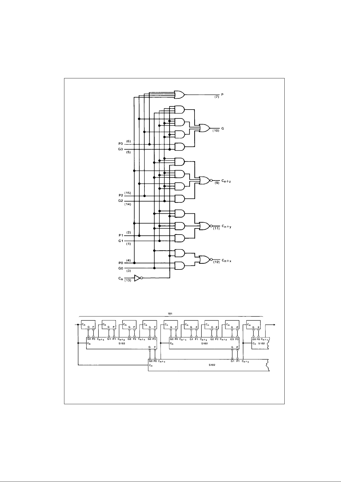
look-ahead packages up to n-bits. The method of casca ding circuits to perform multi-level look-ahead is illustrated
under typical application data.
Carry input and output of the ALU’s are in their true for m,
and the carry propaga te (P) and carry ge nerate (G) ar e in
negated form; therefor e, the carry functions (inputs, out-
puts, generate, and propagate) of the look-ahead generators are implemented in the compatible forms for direct
connection to the ALU. Reinterpretations of carry functions,
as explained on th e 181 data sheet are also applic able to
and compatible with the look-ahead generator. Positive
logic equations for the DM74S182 are:
C
n + x
= G0 + P0 C
n
C
n + y
= G1 + P1 G0 + P1 P0 C
n
C
n + z
= G2 + P2 G1 + P2 P1 G0 + P2 P1 P0 C
n
G = G3 (P3 + G2) (P3 + P2 + G1)
(P
3 + P2 + P1 + G0)
P
= P3 P2 P1 P0
Features
■ Typical propagation delay time 7 ns
■ Typical power dissipation 260 mW
Ordering Code:
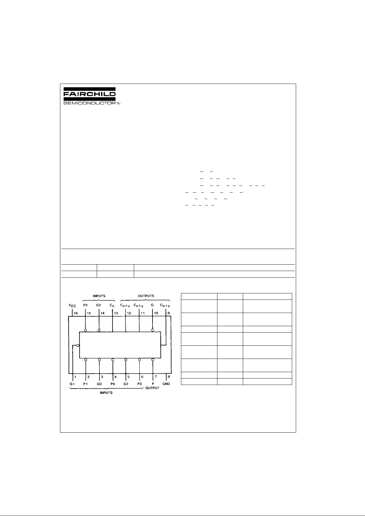
Connection Diagram Pin Designations
Order Number Package Number Package Description
DM74S182N N16E 16-Lead Plastic Dual-In-Line Package (PDIP), JEDEC MS-001, 0.300 Wide
Designation Pin Nos. Function
G0, G1, G2, G3 3, 1, 14, 5 Active LOW
Carry Generate Inputs
P0, P1, P2, P3 4, 2, 15, 6 Active LOW
Carry Propagate Inputs
C
n
13 Carry Input
C
n + x
, C
n + y
, 12, 11, 9 Carry Outputs
C
n + z
G 10 Active LOW
Carry Generate Output
P 7 Active LOW
Carry Propagate Output
V
CC
16 Supply Voltage
GND 8 Ground

www.fairchildsemi.com 2
DM74S182
Logic Diagram
VCC = PIN 16
GND = PIN 8
Typical Application
64-Bit ALU, Full-Carry Look Ahead in Three Levels
A and B inputs, and F out puts of 181 are not shown.
 Loading...