

Fairchild Semiconductor DM74S174N Datasheet
DM74S174 • DM74S175
Hex/Quad D Flip-Flop with Clear
DM74S174 • DM74S175 Hex/Quad D Flip-Flop with Clear
August 1986
Revised April 2000
General Description
These positive-edge-triggered flip-flops utilize TTL circuitry
to implement D-type flip-flop logic. All have a direct clear
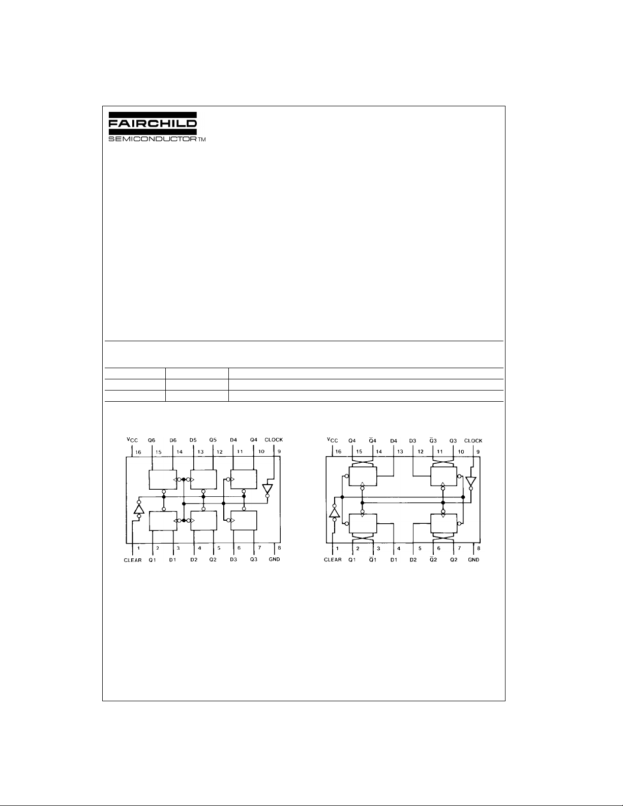
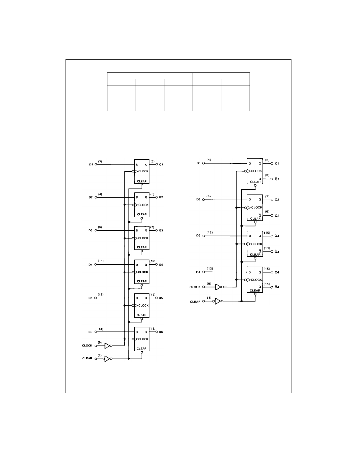
input, and the quad (DM74S 175) vers ions feature co mplementary outputs from each flip-flop.
Information at the D in put s m ee ti ng the se tup tim e requirements is transferred t o the Q output s on the posi tive-go ing
edge of the clock pulse. Clock trigg er ing occ urs a t a par ticular voltage level and is not directly related to the transition
time of the positive-goi ng pulse . When the clock in put is at
either the HIGH or LOW l evel, the D input signal has no
effect at the output.
Features
■ DM74S174 contain six flip-flops with single-rail outputs.
■ DM74S175 contain four flip-flops with double-rail out-
puts.
■ Buffered clock and direct clear inputs
■ Individual data input to each flip-flop
■ Applications include:
Buffer/storage registers
Shift registers
Pattern generators
■ Typical clock frequency 110 MHz
■ Typical power dissipation per flip-flop 75mW
Ordering Code:
Order Number Package Number Package Description
DM74S174N N16E 16-Lead Plastic Dual-In-Line Package (PDIP), JEDEC MS-001, 0.300 Wide
DM74S175N N16E 16-Lead Plastic Dual-In-Line Package (PDIP), JEDEC MS-001, 0.300 Wide
Connection Diagrams
DM74S174 DM74S175
© 2000 Fairchild Semiconductor Corporation DS006472 www.fairchildsemi.com
Function Table (Each Flip-Flop)
Inputs Outputs
Clear Clock D Q Q
LXXLH
H ↑ HHL
H ↑ LLH
HLXQ
H = HIGH Level (steady state)
L = LOW Level (stea dy s t ate)
X = Don’t Care
↑ = Transition from LOW-to-HIGH lev el
DM74S174 • DM74S175
Q0 = The level of Q before the indicated steady-state input conditions were established.
Note 1: DM74S175 only.
Logic Diagrams
DM74S174 DM74S175
(Note 1)
0
Q
0
www.fairchildsemi.com 2
 Loading...