

Fairchild Semiconductor DM74S112N, DM74S112CW Datasheet
© 2000 Fairchild Semiconductor Corporation DS006459 www.fairchildsemi.com
August 1986
Revised April 2000
DM74S112 Dual Negative-Edge-T riggered Master-Slave J-K Flip-Flop with Preset, Clear, and Complementary
Outputs
DM74S112
Dual Negative-Edge-T riggered Master-Sl ave J-K Flip-Flop
with Preset, Clear, and Complementary Outputs
General Description
This device contains two indepe ndent negative-edge-triggered J-K flip-flops with complementary outputs. The J and
K data is processed by the flip -flops on the f alling edge of
the clock pulse. The clock triggering occurs at a voltage
level and is not directly related to the transition time of t he
negative going edge of the clock pulse. Data on the J and
K inputs can be changed while the clock is HIGH or LOW
without affecting the outputs as long as setup and hold
times are not violated. A low logic leve l on the preset or
clear inputs will set or reset the outputs regardless of the
logic levels of the other inputs.
Ordering Code:
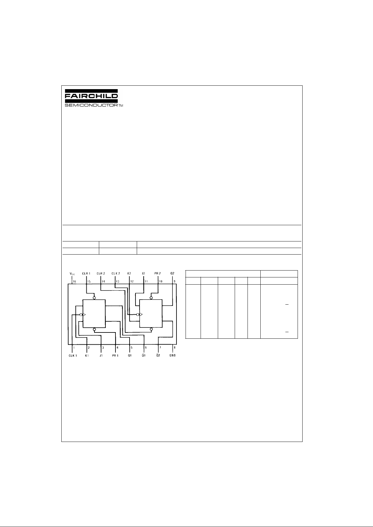
Connection Diagram Function Table
H = HIGH Logic Level
X = Either LOW or HIGH Logic Level
L = LOW Logic Level
↓ = Negative going edge of pulse.
Q0 = The output logic level of Q before the indicated input conditions were
established.
* = This configuration is nonstable ; th at is , it will not persist w hen either the
preset and/or clear in puts return to its inactive (H I GH ) level.
Tog gle = Each output changes to the complement of its previous level on
each falling edge of th e c loc k pulse.
Order Number Package Number Package Description
DM74S112 N16E 16-Lead Plastic Dual-In-Line Package (PDIP), JEDEC MS-001, 0.300 Wide
Inputs Outputs
PR CLR CLK J K Q Q
LHXXXH L
HL XXXL H
LLXXXH*H*
HH ↓ LL Q
0
Q
0
HH ↓ HL H L
HH ↓ LH L H
HH ↓ H H Toggle
HHHXXQ
0
Q
0
www.fairchildsemi.com 2
DM74S112
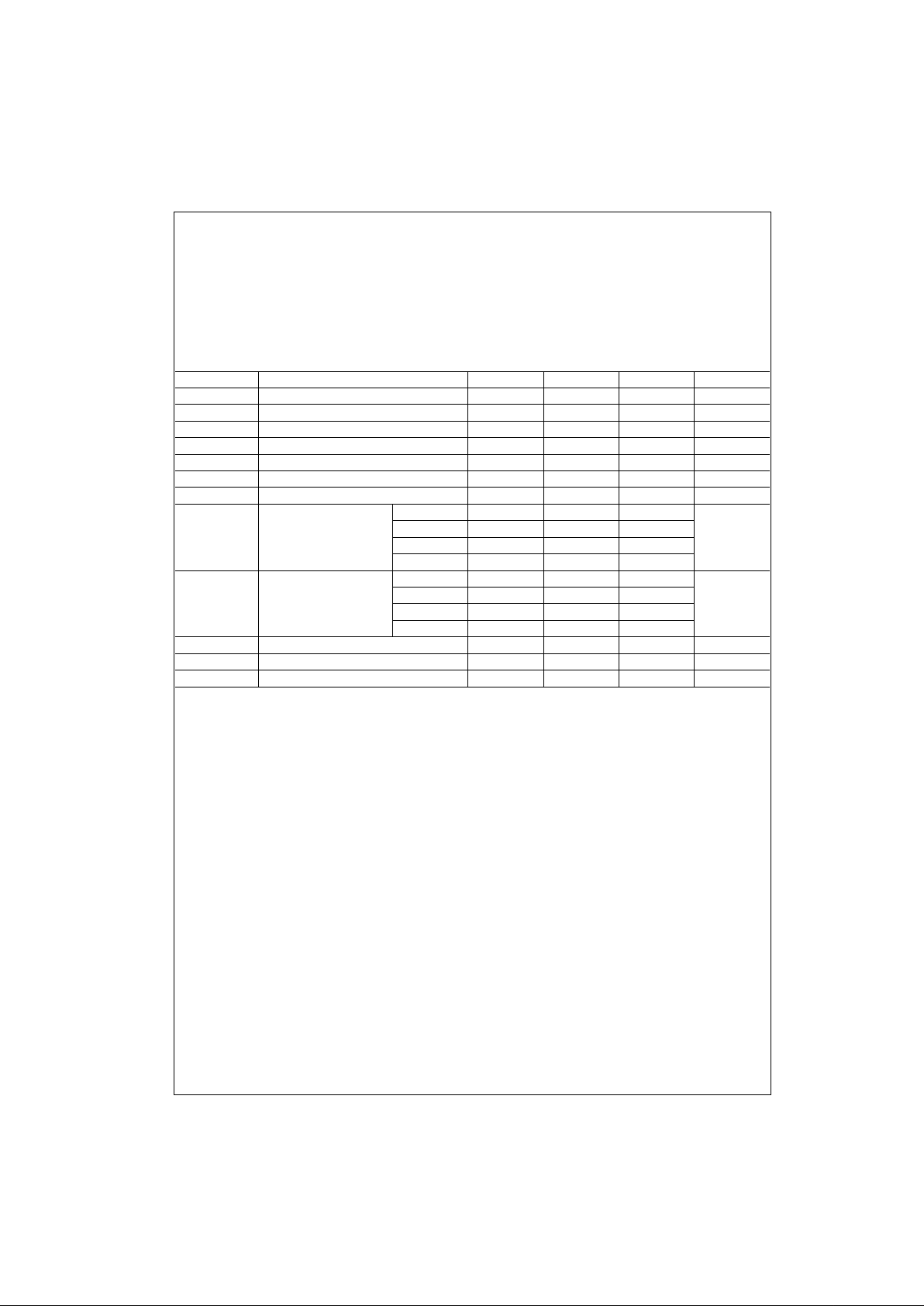
Absolute Maximum Ratings(Note 1)
Note 1: The “Absolute Maxim um Ratin gs” are those valu es beyon d which
the safety of the dev ice cannot be guaranteed. T he device sh ould not be
operated at these limit s. The parametric values defin ed in the Electrical
Characteristics tables are not guaranteed at the absolute maximum ratings.
The “Recommend ed O peratin g Cond itions” t able w ill defin e the co ndition s
for actual device operation.
Recommended Operating Conditions
Note 2: CL = 15 pF, RL = 280Ω, TA = 25°C and VCC = 5V.
Note 3: C
L
= 50 pF, RL = 280Ω, TA = 25°C and VCC = 5V.
Note 4: T
A
= 25°C and VCC = 5V.
Note 5: The symbol (↓) indicates the falling edge at the clock pulse is used for reference.
Supply Voltage 7V
Input Voltage 5.5V
Operating Free Air Temperature Range 0°C to +70°C
Storage Temperature Range −65°C to +150°C
Symbol Parameter Min Nom Max Units
V
CC
Supply Voltage 4.75 5 5.25 V
V
IH
HIGH Level Input Voltage 2 V
V
IL
LOW Level Input Voltage 0.8 V
I
OH
HIGH Level Output Current −1mA
I
OL
LOW Level Output Current 20 mA
f
CLK
Clock Frequency (Note 2) 0 125 80 MHz
f
CLK
Clock Frequency (Note 3) 0 80 60 MHz
t
W
Pulse Width Clock HIGH 6
(Note 2) Clock LOW 6.5
ns
Clear LO W 8
Preset LOW 8
t
W
Pulse Width Clock HIGH 8
(Note 3) Clock LOW 8
ns
Clear LO W 10
Preset LOW 10
t
SU
Setup Time (Note 4)(Note 5) 7↓ ns
t
H
Input Hold Time (Note 4)(Note 5) 0↓ ns
T
A
Free Air Operating Temperature 0 70 °C
 Loading...