

Fairchild Semiconductor DM74ALS1005N, DM74ALS1005MX, DM74ALS1005M Datasheet
© 2000 Fairchild Semiconductor Corporation DS006253 www.fairchildsemi.com
September 1986
Revised February 2000
DM74ALS1005 Hex Inverting Driver with Open Collector Outputs
DM74ALS1005
Hex Inverting Driver with Open Collector Outputs
General Description
These devices contain six independent drivers, each of
which performs the logic INVERT/Complement function.
The outputs require external pull-up resistors for proper
logical operation. The DM74ALS1005 is a d river v ersi o n of
the DM74ALS05A.
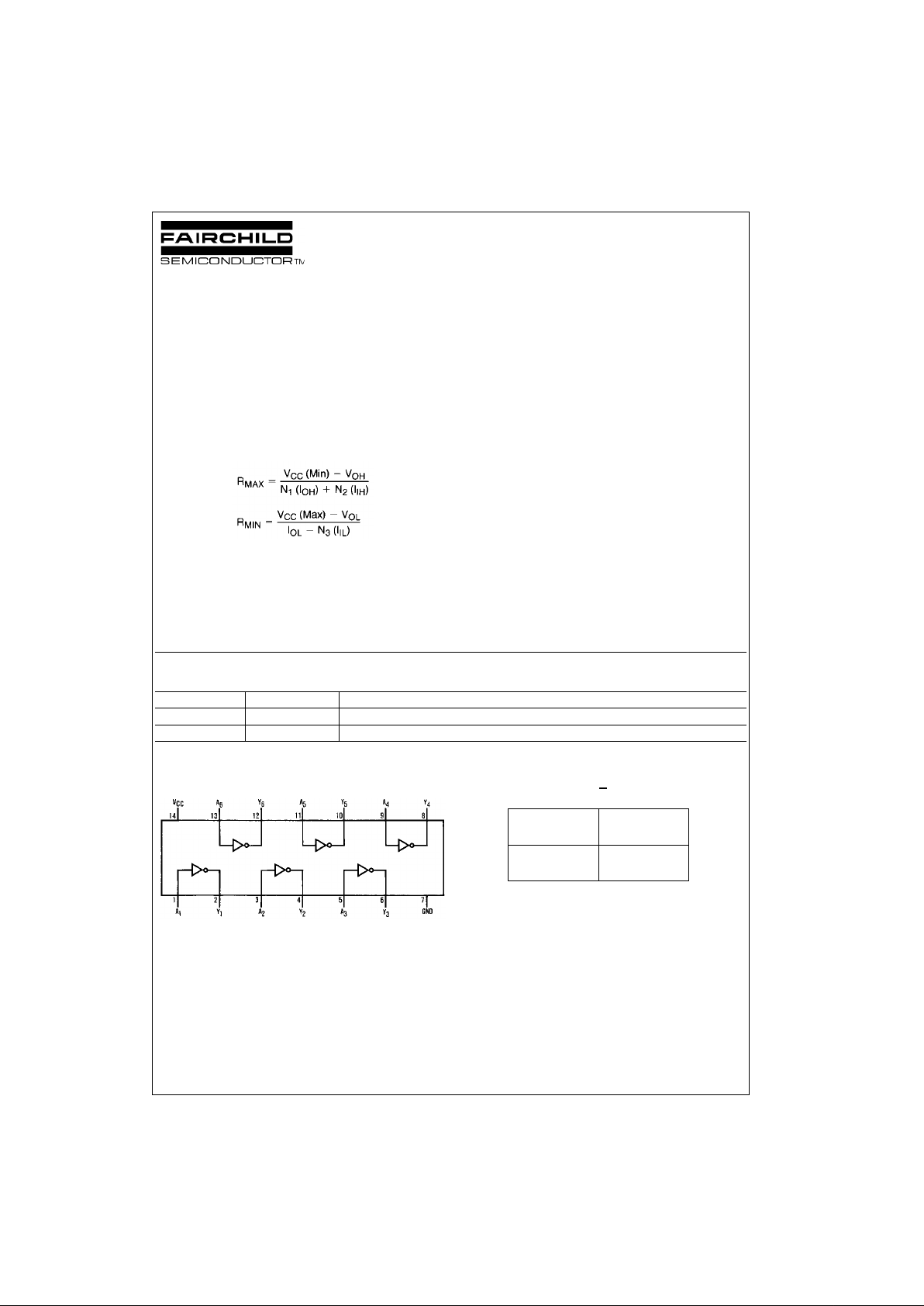
Pull-Up Resistor Equations
Where: N
1
(IOH) = total maximum o utput high cu rrent
for all outputs tied to pull-up resistor
N
2
(IIH) = total maximum input high current for
all inputs tied to pull-up resistor
N
3
(IIL) = total maximum input low current for
all inputs tied to pull-up resistor
Features
■ Switching specifications at 50 pF
■ Switching specifications guaranteed over full tempera-
ture and V
CC
range
■ Advanced oxide-isolated, ion-implanted Schottky TTL
process
■ Functionally and pin for pin compatible with Schottky
and low power Schottky TTL counterpart
■ Improved AC performance over Schottky and low power
Schottky counterparts
Ordering Code:
Devices also availab le in Tape and Reel. Specify by appending th e s uffix let t er “X” to the ordering code.
Connection Diagram Function Table
Y = A
L = LOW Logic Level
H = HIGH Logic Level
Order Number Package Number Package Description
DM74ALS1005M M14A 14-Lead Small Outline Integrated Circuit (SOIC), JEDEC MS-012, 0.150 Narrow
DM74ALS1005N N14A 14-Lead Plastic Dual-In-Line Package (PDIP), JEDEC MS-001, 0.300 Wide
Input Output
AY
HL
LH
www.fairchildsemi.com 2
DM74ALS1005
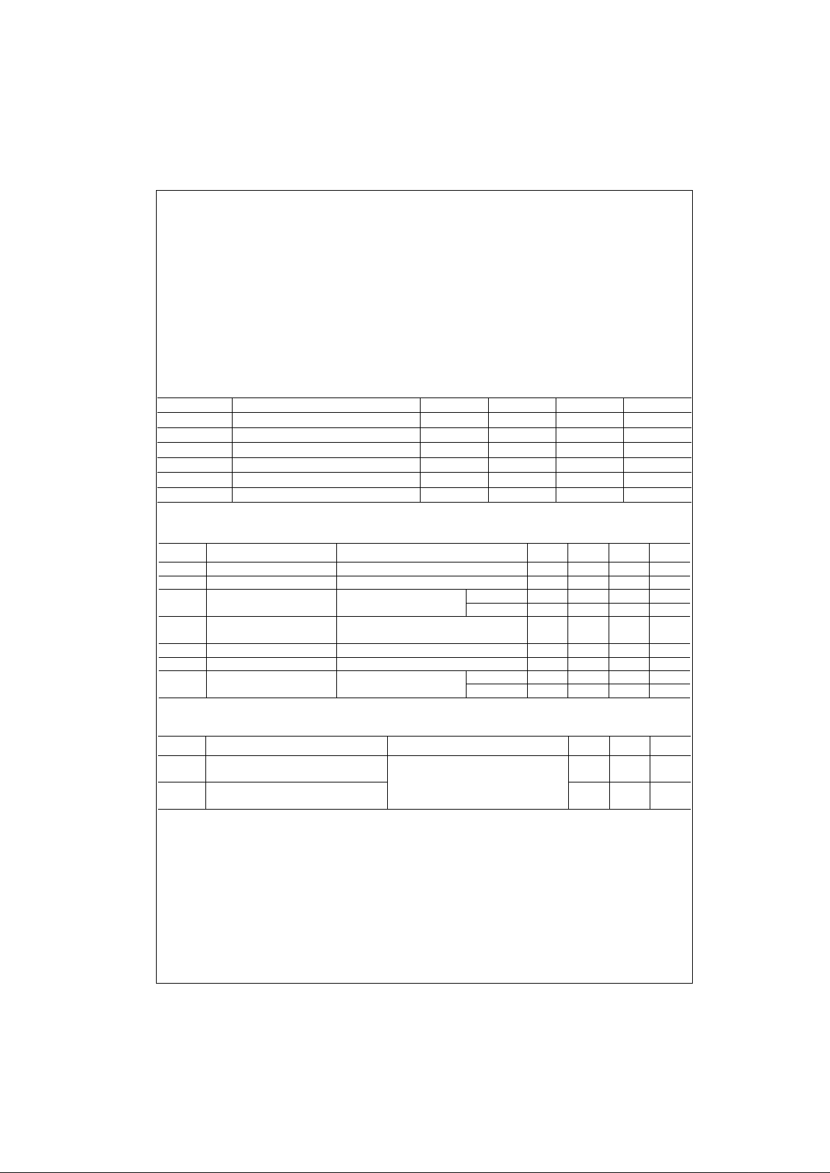
Absolute Maximum Ratings(Note 1)
Note 1: The “Absolute Maximum Ratings” are those values beyond which
the safety of the dev ice cannot be guaranteed. T he device sh ould not be
operated at these limits. The parametric values defined in the Electrical
Characteristics tables are not guaranteed at the absolute maximum ratings.
The “Recommend ed O peratin g Cond itions” t able w ill defin e the co ndition s
for actual device operation.
Recommended Operating Conditions
Electrical Characteristics
over recommended operating free air temperature range. All typical values are measured at VCC = 5V, TA = 25°C.
Switching Characteristics
over recommended operating free air temperature range
Supply Voltage 7V
Input Voltage 7V
OFF-State Output Voltage 7V
Operating Free Air Temperature Range 0°C to +70°C
Storage Temperature Range −65°C to +150°C
Typical θ
JA
N Package 76.0°C/W
M Package 106.5°C/W
Symbol Parameter Min Nom Max Units
V
CC
Supply Voltage 4.5 5 5.5 V
V
IH
HIGH Level Input Voltage 2 V
V
IL
LOW Level Input Voltage 0.8 V
V
OH
HIGH Level Output Voltage 5.5 V
I
OL
LOW Level Output Current 24 mA
T
A
Free Air Operating Temperature 0 70 °C
Symbol Parameter Conditions Min Typ Max Units
V
IK
Input Clamp Voltage VCC = 4.5V, II = −18 mA −1.5 V
I
OH
HIGH Level Output Current VCC = 4.5V, VOH = 5.5V 100 µA
V
OL
LOW Level VCC = 4.5V IOL = 12 mA 0.25 0.4 V
Output Voltage IOL = 24 mA 0.35 0.5 V
I
I
Input Current at Maximum
VCC = 5.5V, VIH = 7V 0.1 mA
Input Voltage
I
IH
HIGH Level Input Current VCC = 5.5V, VIH = 2.7V 20 µA
I
IL
LOW Level Input Current VCC = 5.5V, VIL = 0.4V −0.1 mA
I
CC
Supply Current VCC = 5.5V Outputs HIGH 0.9 3 mA
Outputs LOW 7 12 mA
Symbol Parameter Conditions Min Max Units
t
PLH
Propagation Delay Time VCC = 4.5V to 5.5V
530ns
LOW-to-HIGH Level Output RL = 680Ω
t
PHL
Propagation Delay Time CL = 50 pF
210ns
HIGH-to-LOW Level Output
 Loading...