

Fairchild Semiconductor CD4010CN, CD4010CMX, CD4010CM Datasheet
© 2000 Fairchild Semiconductor Corporation DS005945 www.fairchildsemi.com
October 1987
Revised June 2000
CD4010C Hex Buffers (Non-Inverting)
CD4010C
Hex Buffers (Non-Inverting)
General Description
The CD4010C hex b uffers are monolithic compleme ntary
MOS (CMOS) integrated circuit s. The N- and P-channel
enhancement mode transistors provid e a symmetrical c ircuit with output swings essent ially equ al to the su pply vol tage. This results in high noise immunity over a wide supply
voltage range. No DC power other than that caused by
leakage current is consumed during static conditions. All
inputs are protected agains t static dischar ge. These gates
may be used as hex buffers, CMOS to DTL or TTL interface or as CMOS current drivers. Co nversion ranges are
from 3V to 15V providing V
CC
≤ VDD. The devices also
have buffered outputs which improve tr ansfer character istics by providing very high gain.
Features
■ Wide supply voltage range: 3.0V to 15V
■ Low power: 100 nW (typ.)
■ High noise immunity: 0.45 V
DD
(typ.)
■ High current sinking: 8 mA (min.) at V
O
= 0.5V
capability: and V
DD
= 10V
Applications
• Automotive
• Data terminals
• Instrumentation
• Medical electronics
• Alarm system
• Industrial controls
• Remote metering
• Computers
Ordering Code:
Devices also availab le in Tape and Reel. Specify by appending th e s uffix let t er “X” to the ordering code.
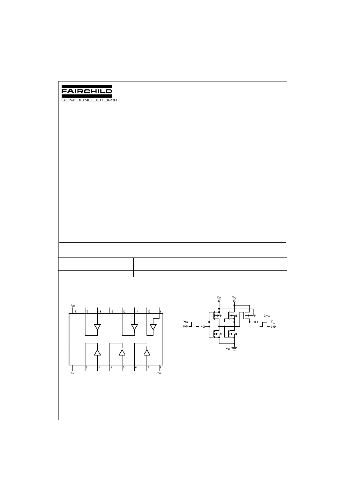
Connection Diagram
Pin Assignments for DIP and SOIC
Top View
Schematic Diagram
Hex COS/MOS to DTL or TTL
converter (inverting).
Connect V
CC
to DTL or TTL suppl y.
Connect V
DD
to COS/MOS supply.
Order Number Package Number Package Description
CD4010CM M16A 16-Lead Small Outline Integrated Circuit (SOIC), JEDEC MS-012, 0.150” Narrow
CD4010CN N16E 16-Lead Plastic Dual-In-Line Package (PDIP), JEDEC MS-001, 0.300” Wide

www.fairchildsemi.com 2
CD4010C
Absolute Maximum Ratings(Note 1)
Note 1: “Absolute Maximum Ratings indicate limits beyond which damage
to the device may occur. Operating Ratings indicate conditions for which
the device is functional, but do not guarantee specific performance limits.”
Note 2: This device should not be connected to circuits with the power on
because high transient voltage may cause permanent damage.
DC Electrical Characteristics
Note 3: IDN and IDP are tested one output at a time.
Voltage at Any Pin (Note 2) VSS − 0.3V to VSS +15.5V
Operating Temperature Range
−45°C to +85°C
Storage Temperature Range (T
S
) −65°C to +150°C
Power Dissipation (P
D
)
Dual-In-Line 700 mW
Small Outline 500 mW
Lead Temperature (T
L
)
(Soldering, 10 seconds) 260
°C
Operating Range (V
DD
)V
SS
+ 3V to VSS + 15V
Test Conditions Limits
Symbol Characteristics (Volts) −40°C +25°C +85°CUnits
V
O
V
DD
Min Max Min Typ Max Min Max
I
CC
Quiescent Device 5 3 0.03 3 42 µA
Current 10 5 0.05 5 70 µA
P
D
Quiescent Device 5 15 0.15 15 210 µW
Dissipation/Package 10 50 0.5 50 700 µW
Output Voltage 5 0.01 0 0.01 0.05 V
V
OL
LOW Level 10 0.01 0 0.01 0.05 V
V
OH
HIGH Level 5 4.99 4.99 5 4.95 V
10 9.99 9.99 10 9.95 V
Noise Immunity
(All Inputs)
V
NL
VO ≥ 1.5 5 1.6 1.5 2.25 1.4 V
V
O
≥ 3.0 10 3.2 3 4.5 2.9 V
V
NH
VO ≥ 3.5 5 1.4 1.5 2.25 1.5 V
V
O
≥ 7.0 10 2.9 3 4.5 3 V
Output Drive Current 0.4 5 3.6 3 2.4 mA
I
D
N N-Channel (Note 3) 0.5 10 9.6 8 6.4 mA
I
D
P P-Channel (Note 3) 2.5 5 −1.5 −1.25 −1mA
9.5 10 −0.72 −0.6 −0.48 mA
I
IN
Input Current 10 pA
 Loading...