Fairchild Semiconductor CD4007CN, CD4007CMX, CD4007CM Datasheet

October 1987
Revised January 1999
CD4007C Dual Complementary Pair Plus Inverter
© 1999 Fairchild Semiconductor Corporation DS005943.prf www.fairchildsemi.com
CD4007C
Dual Complementary Pair Plus Inverter
General Description
The CD4007C consists of three comp l ementary pairs of Nand P-channel enha ncement mode MOS transis tors suitable for series/shunt appli cations. All inputs ar e protected
from static discharge by diode clamps to V
DD
and VSS.
For proper operation the voltages at all pins must be constrained to be between V
SS
− 0.3V and VDD + 0.3V at all
times.
Features
■ Wide supply voltage range: 3.0V to 15V
■ High noise immunity: 0.45 V
CC
(typ.)
Ordering Code:
Devices also available in Tape and Reel. Specify by appending the suffix letter “X” to the ordering code.
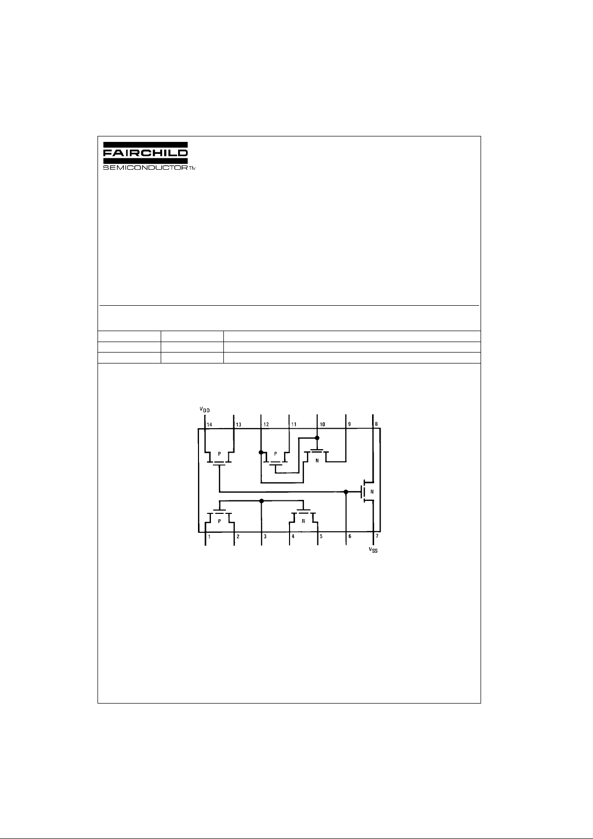
Connection Diagram
Pin Assignments for DIP and SOIC
Note: All P-channel subst rat es are connected to VDD and all N-channel substrates are connected to VSS.
Top View
Order Number Package Number Package Description
CD4007CM M14A 14-Lead Small Outline Integrated Circuit (SOIC), JEDEC MS-120, 0.150” Narrow
CD4007CN N14A 14-Lead Plastic Dual-In-Line Package (PDIP), JEDEC MS–001, 0.300” Wide

www.fairchildsemi.com 2
CD4007C
Absolute Maximum Ratings(Note 1)
Note 1: This device should not be connected to circuits with the power on
because high transie nt voltages may cause permanent damage.
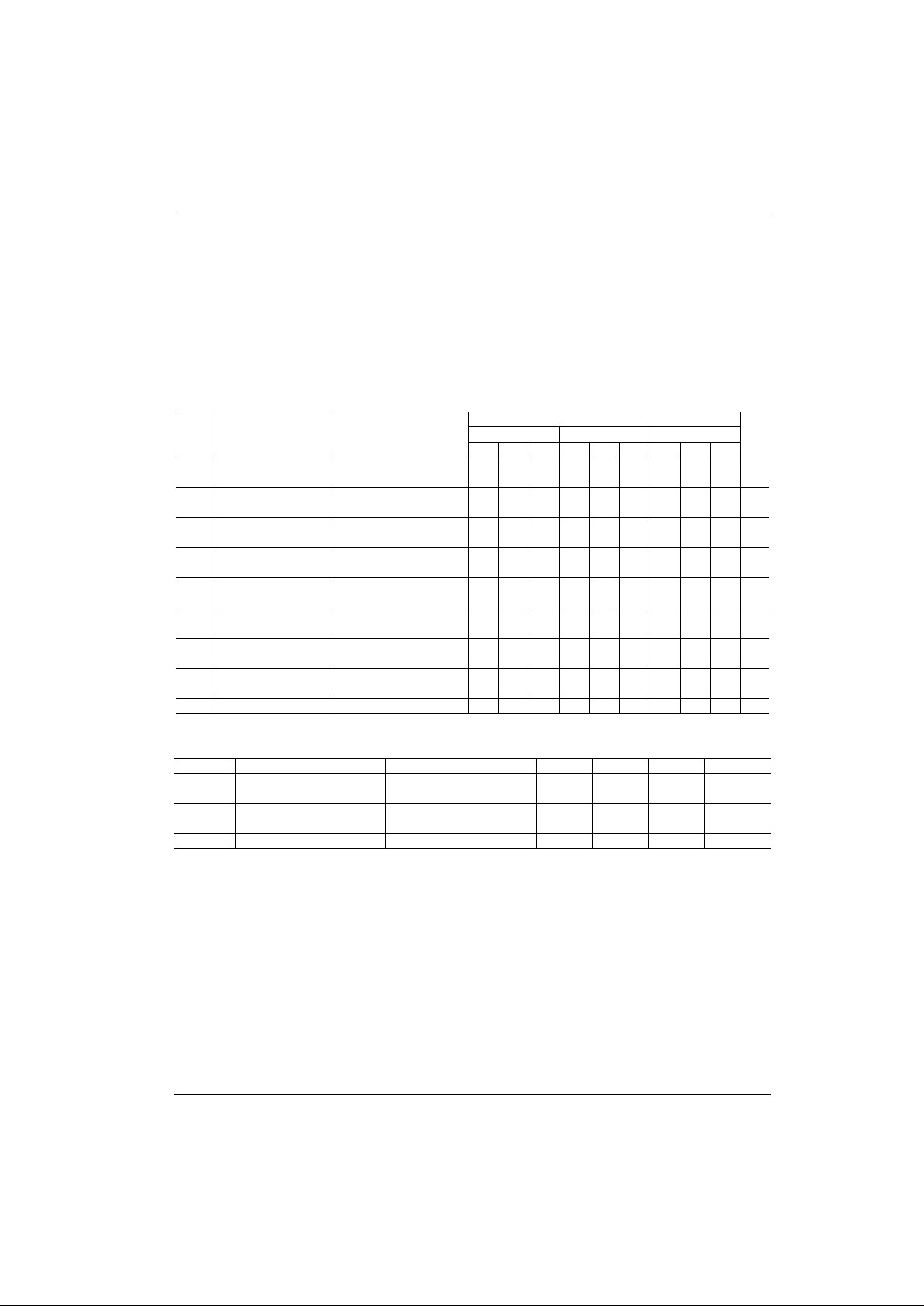
DC Electrical Characteristics
AC Electrical Charac teristics
(Note 2)
T
A
= 25°C and CL = 15 pF and rise and fall t imes = 20 ns. Typical temperature coefficient for all values of VDD = 0.3%/°C
Note 2: AC Parameters are guara nt eed by DC correlated testing.
Voltage at Any Pin VSS −0.3V to VDD +0.3V
Operating Temperature Range −40°C to +85°C
Storage Temperature Range −65°C to +150°C
Power Dissipation (P
D
)
Dual-In-Line 700 mW
Small Outline 500 mW
Operating V
DD
Range VSS +3.0V to VSS +15V
Lead Temperature
(Soldering, 10 seconds) 260°C
Limits
Symbol Parameter Conditions −40°C +25°C +85°CUnits
Min Typ Max Min Typ Max Min Typ Max
I
L
Quiescent Device VDD = 5.0V 0.5 0.005 0.05 15 µA
Current VDD = 10V 1.0 0.005 1.0 30 µA
P
D
Quiescent Device VDD = 5.0V 2.5 0.025 2.5 75 µW
Dissipation Package VDD = 10V 10 0.05 10 300 µW
V
OL
Output Voltage VDD = 5.0V 0.05 0 0.01 0.05 V
LOW Level VDD = 10V 0.05 0 0.01 0.05 V
V
OH
Output Voltage VDD = 5.0V 4.95 4.95 5.0 4.95 V
HIGH Level VDD = 10V 9.95 9.95 10 9.95 V
V
NL
Noise Immunity VDD = 5.0V, VO = 3.6V 1.5 2.25 1.5 1.4 V
(All inputs) VDD = 10V, VO = 7.2V 3.0 4.5 3.0 2.9 V
V
NH
Noise Immunity VDD = 5.0V, VO = 0.95V 3.6 3.5 2.25 3.5 V
(All Inputs) VDD = 10V, VO = 2.9V 7.1 7.0 4.5 7.0 V
IDN Output Drive Current VDD = 5.0V, VO = 0.4V, VI = VDD0.35 0.3 1.0 0.24 mA
N-Channel VDD = 10V, VO = 0.5V, VI = VDD1.2 1.0 2.5 0.8 mA
IDP Output Drive Current VDD = 5.0V, VO = 2.5V, VI = VSS−1.3 −1.1 −4.0 −0.9 mA
P-Channel VDD = 10V, VO = 9.5V, VI = VSS−0.65 −0.55 −2.5 −0.45 mA
I
I
Input Current 10 pA
Symbol Parameter Conditions Min Typ Max Units
t
PLH
= t
PHL
Propagation Delay Time VDD = 5.0V 35 75 ns
VDD = 10V 20 50 ns
t
TLH
= t
THL
Transition Time VDD = 5.0V 50 100 ns
VDD = 10V 30 50 ns
C
I
Input Capacitance Any Input 5 pF
 Loading...