Fairchild Semiconductor 74LVTH646WMX, 74LVTH646WM, 74LVTH646MTCX, 74LVTH646MTC Datasheet

© 2000 Fairchild Semiconductor Corporation DS012017 www.fairchildsemi.com
November 1999
Revised May 2000
74LVTH646 Low Voltage Octal Transceiver/Register with 3-STATE Outputs
74LVTH646
Low Voltage Octal Transcei ver/Register
with 3-STATE Outputs
General Description
The LVTH646 consists of registered b us transceiver circuits, D-type flip-flops, and control circuitry providing multiplexed transmission of data directly fr om the input bus or
from the internal st orage regi sters. Data o n the A or B bus
will be loaded into the respective registers on the LOW-toHIGH transition of the appropriate clock pin (CPAB or
CPBA). (See Functional Description)
The LVTH646 data inputs include b ushold, elim inating the
need for external pull-up resistors to hold unused inputs.
The bus transceivers are d esigned for low-voltage (3.3V)
V
CC
applications, but with the capability to provide a TTL
interface to a 5V environmen t. The LVTH646 is fabricated
with an advanced BiCMOS technology to achieve high
speed operation similar to 5V ABT while maintaining low
power dissipation.
Features
■ Input and output interface capability to systems at
5V V
CC
■ Bushold data inputs eliminate the need for external
pull-up resistors to hold unused inputs
■ Live insertion/extraction per mitted
■ Power Up/Down high impedance provides glitch-free
bus loading
■ Outputs source/sink −32 mA/+64 mA
■ Functionally compatible with the 74 series 646
■ Latch-up performance exce eds 500 mA
Ordering Code:
Devices also availab le in Tape and Reel. Specify by appending let t er s uffix “X” to the ordering code.
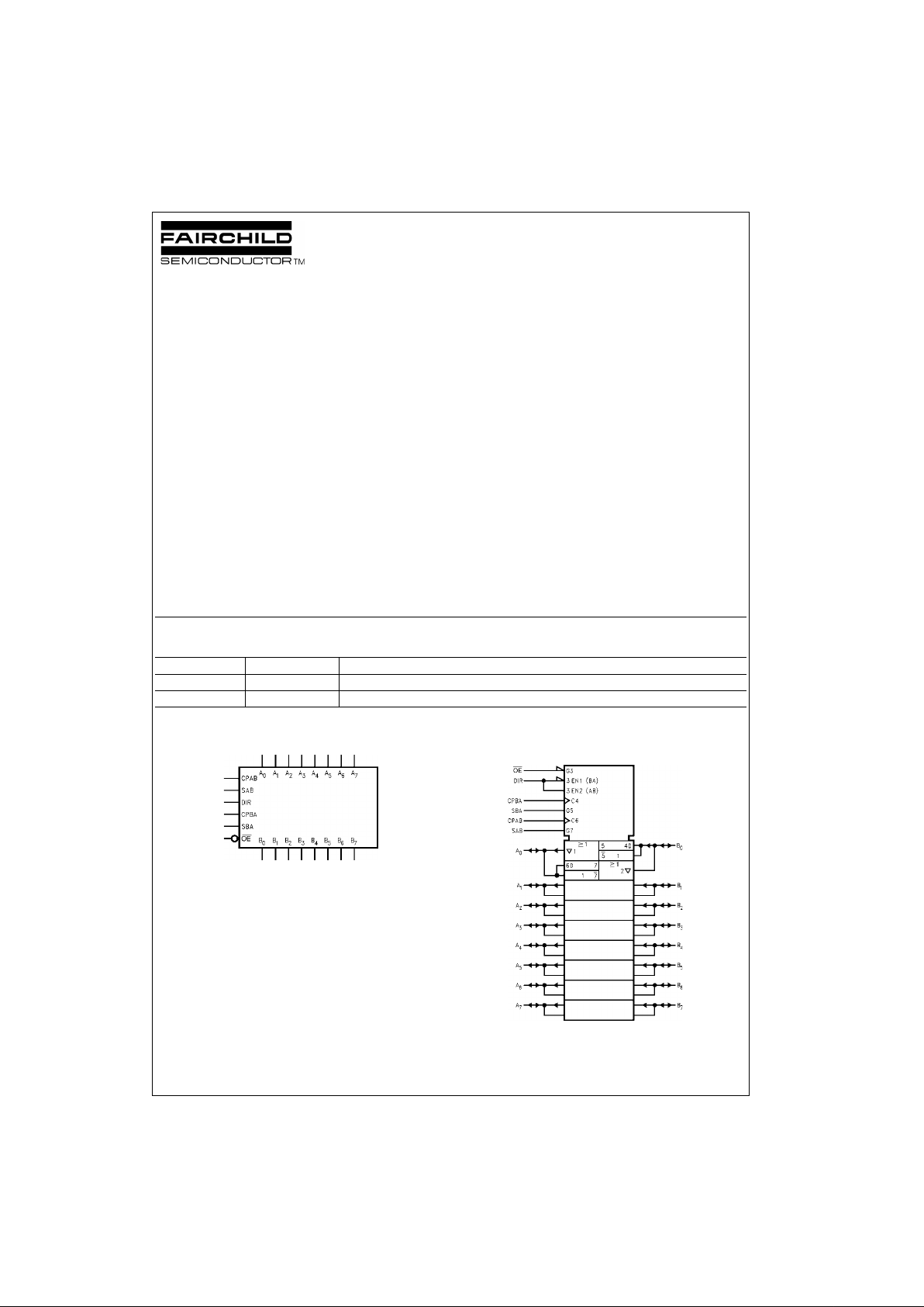
Logic Symbols
IEEE/IEC
Order Number Package Number Package Description
74LVTH646WM M24B 24-Lead Small Outline Integrated Circuit (SOIC), JEDEC MS-013, 0.300” Wide
74LVTH646MTC MTC24 24-Lead Thin Shrink Small Outline Package (TSSOP), JEDEC MO-153, 4.4mm Wide

www.fairchildsemi.com 2
74LVTH646
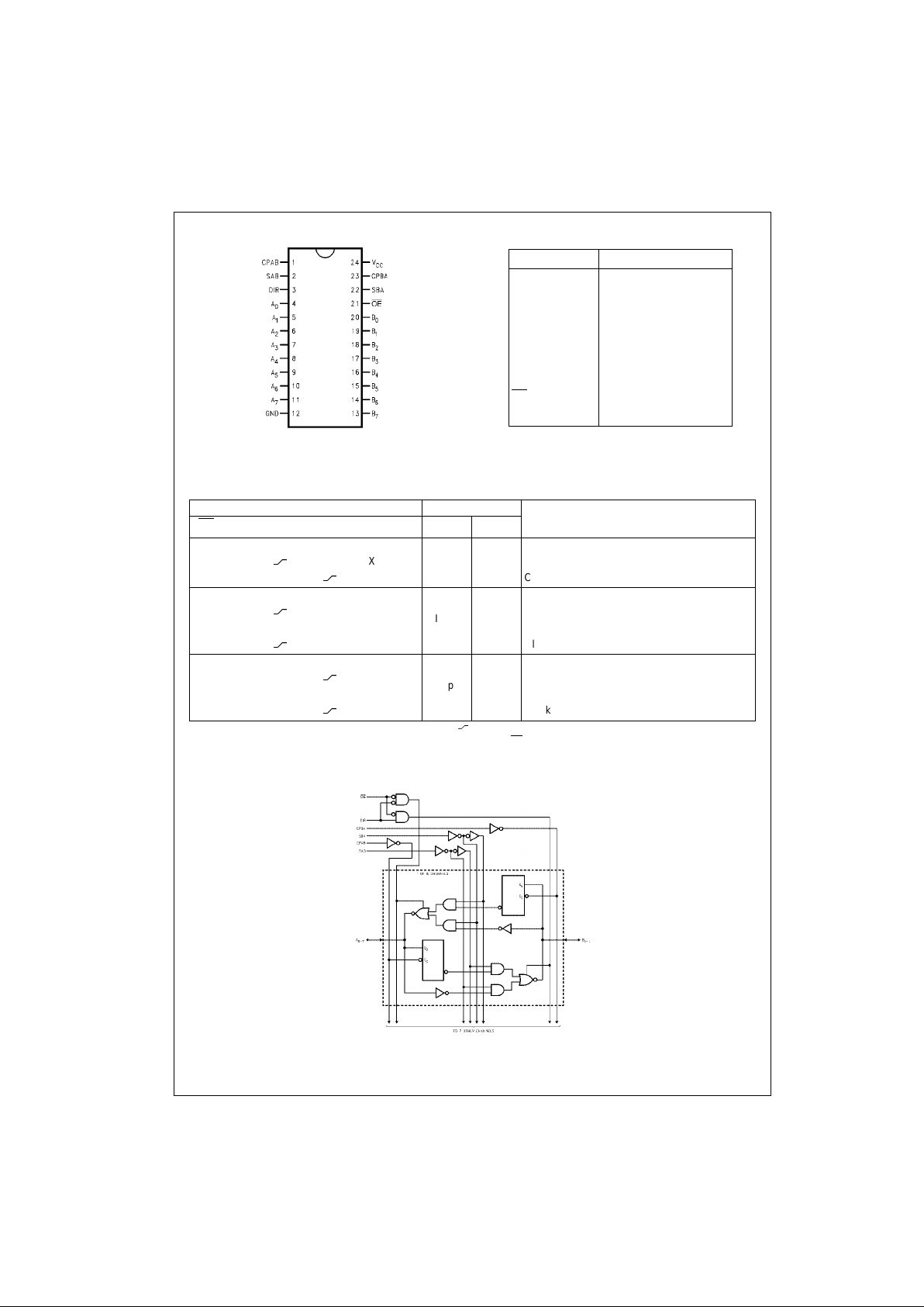
Connection Diagram Pin Descriptions
Truth Table
(Note 1)
H = HIGH Voltage Level L = LOW Voltage Level X = Immaterial = LOW-to-HIGH Transition
Note 1: The data output func tions m ay be en abled or di sabled by vario us signal s at th e OE
and DIR inputs. Dat a input function s are alwa ys ena bled; i.e. ,
data at the bus pins w ill be stored on every LOW-to -H I GH t ransition of the appropr iat e clock inputs.
Logic Diagram
Please note that this diagram is provided only for the understanding of logic operations and should not be used to estimate propagation delays.
Pin Names Description
A
0–A7
Data Register A Inputs
Data Register A Outputs
B
0–B7
Data Register B Inputs
Data Register B Outputs
CPAB, CPBA Clock Pulse Inputs
SAB, SBA Transmit/Receive Inputs
OE
Output Enable Input
DIR Direction Control Input
Inputs Data I/O
Function
OE
DIR CPAB CPBA SAB SBA A0–A7B0–B
7
H X H or L H or L X X Isolation
HX
X X X Input Input Clock An Data into A Register
HX X
X X Clock Bn Data into B Register
LH X X LX A
n
to Bn—Real Time (Transparent Mode)
LH
XLX
Input Output
Clock An Data into A Register
L H H or L X H X A Register to B
n
(Stored Mode)
LH
X H X Clo ck An Data into A Register and Output to B
n
LL X X XL Bn to An—Real Time (Transparent Mode)
LL X
XL
Output Input
Clock Bn Data into B Register
L L X H or L X H B Register to A
n
(Stored Mode)
LL X
X H Clock Bn Data into B Register and Output to A
n

3 www.fairchildsemi.com
74LVTH646
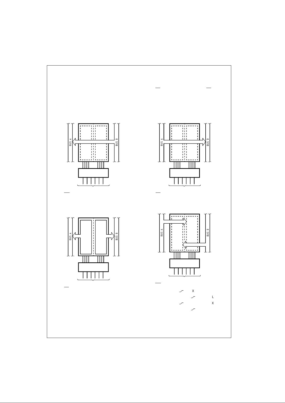
Functional Description
In the transceiver mode , da ta p re sent at th e H I GH imp ed ance po rt m ay b e sto re d i n e ithe r th e A or B re gister or both. The
select (SAB, SBA) controls can multiplex stored and real-time. The exa mples below demonst rate the four f undamenta l busmanagement functions that can be performed.
The direction control (DIR) determines which bus will receive data when OE
is LOW. In the isolation mode (OE HIGH), A
data may be stored in one register an d/or B da ta may be stored i n the othe r register. When an output fun ction is disabled ,
the input function is still enabled and may be used to store and transmit data. Only one of the two busses, A or B, may be
driven at a time.
Real-Time Transfer
Bus B to Bus A
Transfer Storage
Data to A or B
Real-Time Transfer
Bus B to Bus A
Storage
OE
DIR CPAB CPBA SAB SBA
LLXXXL
OE
DIR CPAB CPBA SAB SBA
LLXH or LXH
LHH or LXHX
OE DIR CPAB CPBA SAB SBA
LHXXLX
OE
DIR CPAB CPBA SAB SBA
LH
XLX
LLX
XL
HX
XXX
HXX
XX
 Loading...