Fairchild Semiconductor 74LVTH16652MTDX, 74LVTH16652MTD, 74LVTH16652MEAX, 74LVTH16652MEA Datasheet

© 2000 Fairchild Semiconductor Corporation DS012024 www.fairchildsemi.com
January 2000
Revised January 2000
74LVTH16652 Low Voltage 16-Bit Transceiver/Register with 3-STATE Outputs
74LVTH16652
Low Voltage 16-Bit Transceiver/Register
with 3-STATE Outputs
General Description
The LVTH16652 consists of sixteen bus transceiver circuits
with D-type flip-flops, and control circuitry arranged for multiplexed transmission of data direct ly from the input bus or
from the internal registers. Each byte has separate control
inputs which can be shorte d together for full 16-bit operation. Data on the A or B bus will be clocked into the registers as the appropriat e clock pin goes to the HIGH logic
level. Output Enable pins (OEAB, OEBA
) are provided to
control the transceiver function (see Functional Description).
The LVTH16652 data inputs includ e bushold, eliminating
the need for external pull-up resistors to hold unused
inputs.
The transceivers are d esigned for low-volta ge (3.3V) V
CC
applications, but with the capability to provide a TTL interface to a 5V environment. The LVTH16652 is fab ricated
with an advanced BiCMOS technology to achieve high
speed operation similar to 5V ABT while maintaining low
power dissipation.
Features
■ Input and output interface capability to systems at
5V V
CC
■ Bushold data inputs eliminate the need for external
pull-up resistors to hold unused inputs
■ Live insertion/extraction per mitt ed
■ Power Up/Down high impedance provides glitch-free
bus loading
■ Outputs source/sink −32 mA/+64 mA
■ Functionally compatible with the 74 series 16652
■ Latch-up performance exceeds 500 mA
Ordering Code:
Devices also availab le in Tape and Reel. Specify by appending su ffix let te r “X” to the ordering code.
Order Number Package Number Package Description
74LVTH16652MEA MS56A 56-Lead Shrink Small Outline Package (SSOP), JEDEC MO-118, 0.300 Wide
74LVTH16652MTD MTD56 56-Lead Thin Shrink Small Outline Package (TSSOP), JEDEC MO-153, 6.1mm Wide

www.fairchildsemi.com 2
74LVTH16652
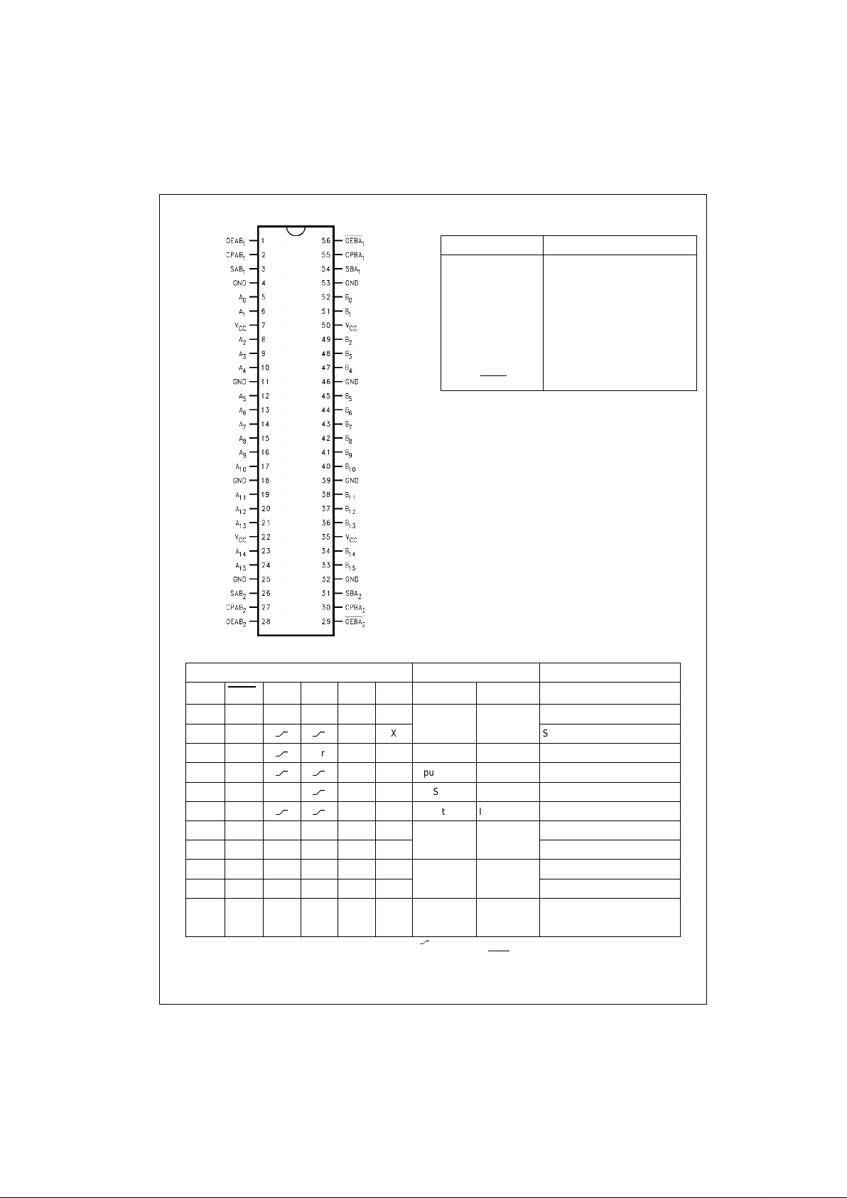
Connection Diagram Pin Descriptions
Truth Table
(Note 1)
H = HIGH Voltage Level L = LOW Voltage Lev el X = Immaterial = LOW-to-HIGH Clock Transition
Note 1: The data output fu nction s may b e enable d or di sabled b y variou s signa ls at OEA B or O EBA
inputs. Data input function s are a lways e nabled, i.e.,
data at the bus pins w ill be stored on every LOW- to -H I GH t ransition on the clock inp ut s . This also applies to data I/O (A and B: 8–15) and #2 cont rol pins
Pin Names Description
A
0–A15
Data Register A Inputs/
3-STATE Outputs
B
0–B15
Data Register B Inputs/
3-STATE Outputs
CPAB
n
, CPBA
n
Clock Pulse Inputs
SAB
n
, SBA
n
Select Inputs
OEAB
n
, OEBA
n
Output Enable Inputs
Inputs Inputs/Outputs Operating Mode
OEAB
1
OEBA1CPAB1CPBA1SAB1SBA1A0 thru A7B0 thru B
7
L H H or L H or L X X Input Input Isolation
LH
X X Store A and B Data
XH
H or L X X Input Not Specified Store A, Hold B
HH
X X Input Output Store A in Both Registers
LXH or L
X X Not Specified Input Hold A, Store B
LL
X X Output Input Store B in Both Registers
L L X X X L Output Input Real-Time B Data to A Bus
L L X H or L X H Store B Data to A Bus
H H X X L X Input Output Real-Time A Data to B Bus
H H H or L X H X Stored A Data to B Bus
H L H or L H or L H H Output Output Stored A Data to B Bus and
Stored B Data to A Bus

3 www.fairchildsemi.com
74LVTH16652
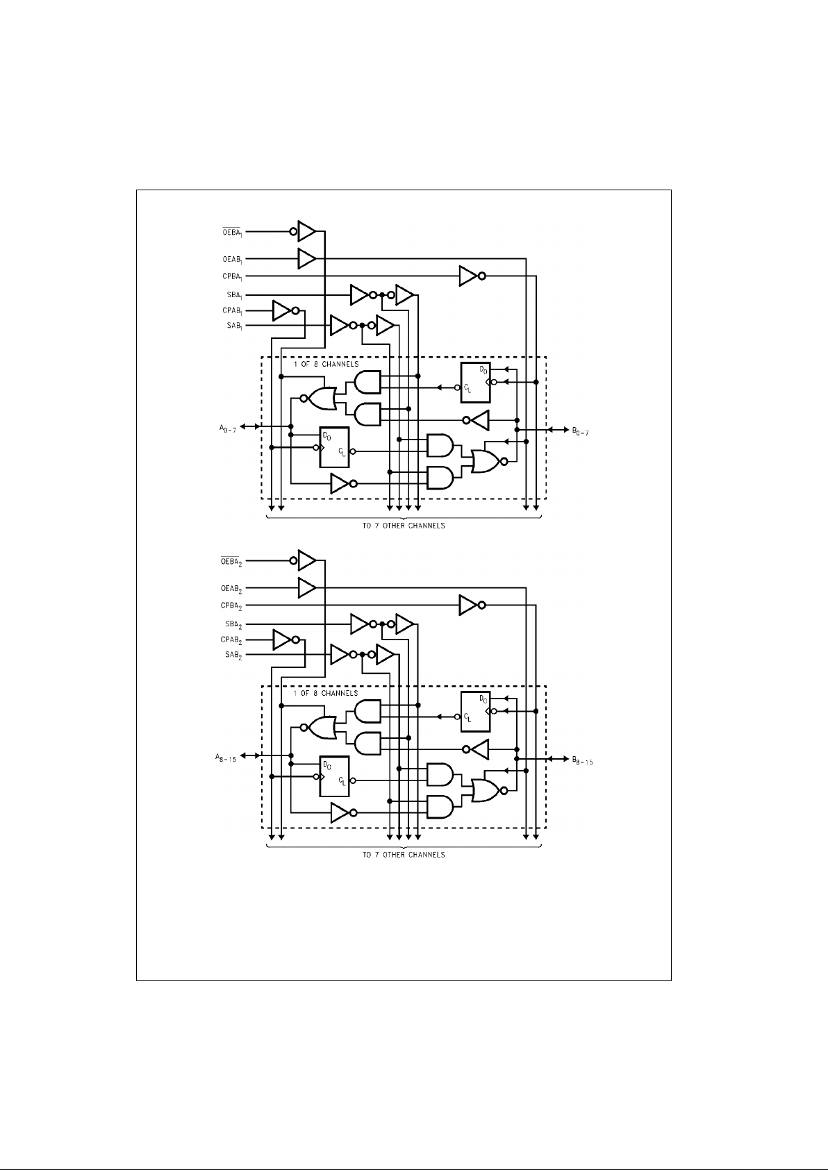
Logic Diagrams
Please note that thes e diagrams are provide d only for the understan ding of logic operations a nd should not be used to es t im ate propagation delays.
 Loading...