Fairchild Semiconductor 74LVTH16543MTDX, 74LVTH16543MTD, 74LVTH16543MEAX, 74LVTH16543MEA Datasheet

© 2000 Fairchild Semiconductor Corporation DS012449 www.fairchildsemi.com
January 2000
Revised January 2000
74LVTH16543 Low Voltage 16-Bit Registered Transceiver with 3-STATE Outputs
74LVTH16543
Low Voltage 16-Bit Registered Transceiver
with 3-STATE Outputs
General Description
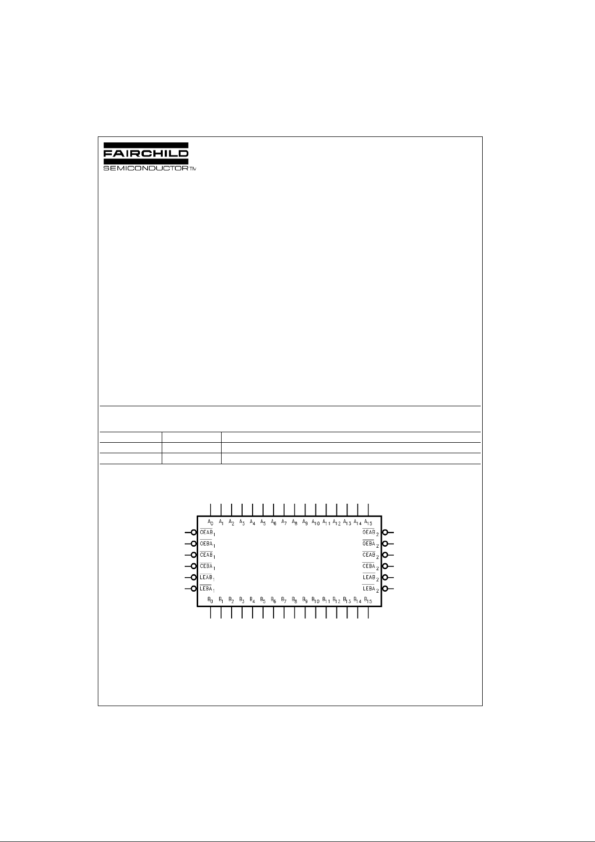
The LVTH16543 16-bit transceiver c ontains two sets of Dtype latches for temporary sto rage o f data flowing in either
direction. Separate Latch Enable and Output Enable inputs
are provided for each reg ister to permit indep endent control of inputting and outputt ing in either direction of data
flow. Each byte has separate control inputs, which ca n be
shorted together for full 16-bit operation.
The LVTH16543 data inputs includ e bushold, eliminating
the need for external pull-up resistors to hold unused
inputs.
These transceivers are designed for low-voltage (3.3V)
V
CC
applications, but with the capability to provide a TTL
interface to a 5V environ ment. The LVTH16543 is fabricated with an advanced BiCMOS technology to achieve
high speed opera tion similar to 5V ABT while maintaining
low power dissipation.
Features
■ Input and output interface capability to systems at
5V V
CC
■ Bushold data inputs elimina te the nee d for exte rnal pul lup resistors to hold unused inputs
■ Live insertion/extraction per mitt ed
■ Power Up/Down high impedance provides glitch-free
bus loading
■ Outputs source/sink −32 mA/+64 mA
■ Functionally compatible with the 74 series 16543
■ Latch-up performance exceeds 500 mA
Ordering Code:
Device also available in Tape and Reel. Specify by appending s uffix let te r “X” to the ordering code.
Logic Symbol
Order Number Package Number Package Description
74LVTH16543MEA MS56A 56-Lead Shrink Small Outline Package (SSOP), JEDEC MO-118, 0.300 Wide
74LVTH16543MTD MTD56 56-Lead Thin Shrink Small Outline Package (TSSOP), JEDEC MO-153, 6.1mm Wide

www.fairchildsemi.com 2
74LVTH16543
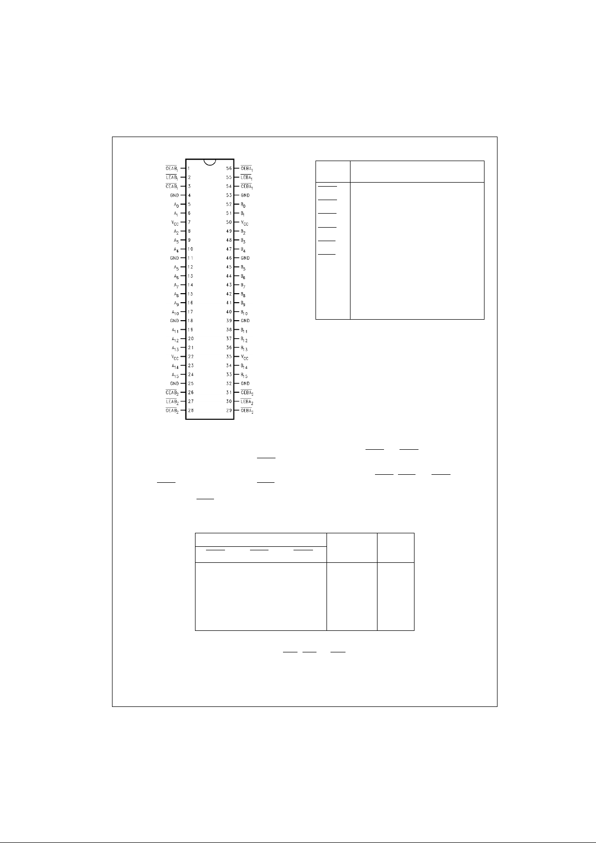
Connection Diagram Pin Descriptions
Functional Description
The LVTH16543 contains two sets of D-type latches, with
separate input and outp ut controls for each. For data flow
from A to B, for example, the A to B Enable (CEAB
) input
must be LOW in order to enter data from the A Port or take
data from the B Port as ind icated in the Data I/ O Control
Table. With CEAB
LOW, a low signal on (LEAB) input
makes the A to B lat ches transparent; a s ubse qu ent L O Wto-HIGH transition of the LEAB
line puts the A latches in
the storage mode and their outputs no longer change with
the A inputs. With CEAB
and OEAB both LOW, the B output buffers are active an d reflect the data prese nt on the
output of the A latches. C ontrol of data flow from B to A is
similar, but using the CEBA
, LEBA and OEBA. Each b yte
has separate control input s, al lowi n g the device to be used
as two 8-bit transceivers or as one 16-bit transceiver.
Data I/O Control Table
H = HIGH Voltage Level
L = LOW Voltage Level
X = Immaterial
A-to-B data flow shown; B-to-A flow control is the same, except using CEBA
n
, LEBAn and OEBA
n
Pin
Names
Description
OEAB
n
A-to-B Output Enable Input (Active LOW)
OEBA
n
B-to-A Output Enable Input (Active LOW)
CEAB
n
A-to-B Enable Input (Active LOW)
CEBA
n
B-to-A Enable Input (Active LOW)
LEAB
n
A-to-B Latch Enable Input (Active LOW)
LEBA
n
B-to-A Latch Enable Input (Active LOW)
A
0–A15
A-to-B Data Inputs or
B-to-A 3-STA TE Outputs
B
0–B15
B-to-A Data Inputs or
A-to-B 3-STA TE Outputs
Inputs Latch Status
(Byte n)
Output
Buffers
(Byte n)
CEAB
n
LEAB
n
OEAB
n
H X X Latched High Z
X H X Latched —
L L X Transparent —
X X H — High Z
L X L — Driving

3 www.fairchildsemi.com
74LVTH16543
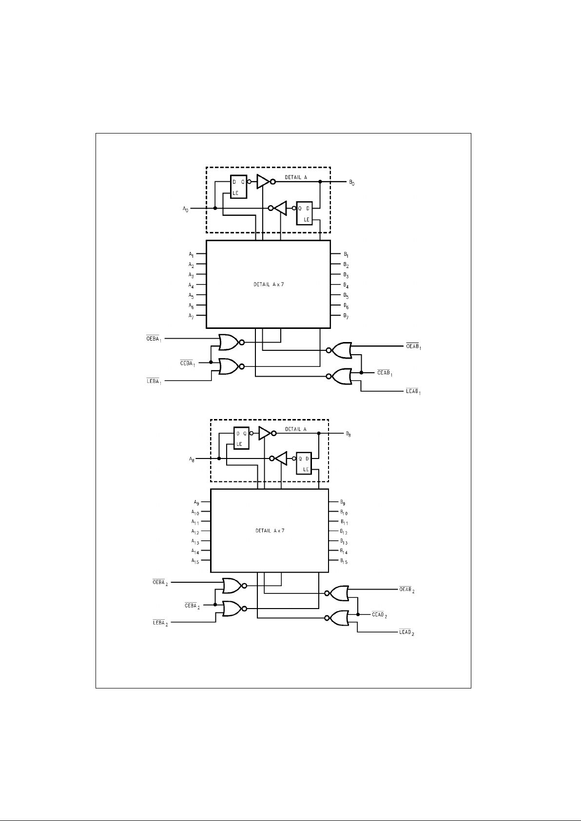
Logic Diagrams
Byte 1 (0:7)
Please note that this d iagram is provided only f or t he understanding of lo gic operations and should not be used to estimat e propagation delays.
Byte 2 (8:15)
Please note that this d iagram is provided only f or t he understanding of lo gic operations and should not be used to estimat e propagation delays.
 Loading...