

Fairchild Semiconductor 74F14SJX, 74F14SJ, 74F14SCX, 74F14SC Datasheet
© 1999 Fairchild Semiconductor Corporation DS009461 www.fairchildsemi.com
March 1988
Revised July 1999
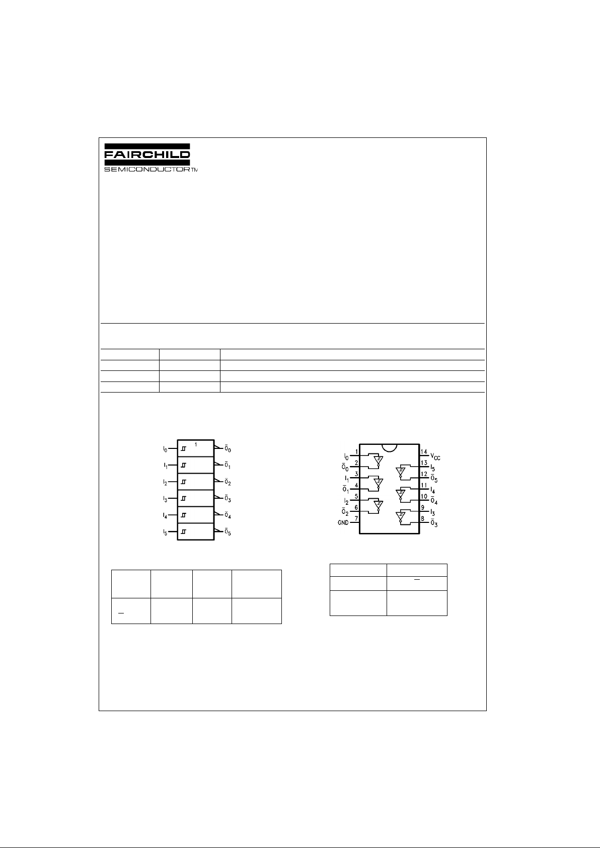
74F14 Hex Inverter Schmitt Trigger
74F14
Hex Inverter Schmitt Trigger
General Description
The 74F14 contains six logic inv erters which accept standard TTL input signa ls and provide standard TTL out put
levels. They are capabl e of transforming slowly ch anging
input signals into sharpl y defined, ji tter-f ree outp ut s ignals .
In addition, they have a greater noise margin tha n conventional inverters.
Each circuit contains a Schmitt trig ger followed by a Da rlington level shifter and a phase splitter driving a TTL
totem-pole out put. The Schmitt trigger uses positive feed
back to effective ly speed- up slow i nput tra nsition, and pr ovide different input threshold voltages for positive and negative-going transitions. This hysteresis between the
positive-going and negative-going input thresholds (typically 800 mV) is determined internally by resistor ratios and
is essentially insensitive to temperature and supply voltage
variations.
Ordering Code:
Devices also available in Tape and Reel. Specify by appending the suffix letter “X” to the ordering code.
Logic Symbol
IEEE/IEC
Unit Loading/Fan Out
Connection Diagram
Function T a ble
H = HIGH Voltage Level
L = LOW Voltage Level
Order Number Package Number Package Description
74F14SC M14A 14-Lead Small Outline Integrated Circuit (SOIC), JEDEC MS-120, 0.150 Narrow
74F14SJ M14D 14-Lead Small Outline Package (SOP), EIAJ TYPE II, 5.3mm Wide
74F14PC N14A 14-Lead Plastic Dual-In-Line Package (PDIP), JEDEC MS-001, 0.300 Wide
Pin Names Description
U.L.
Input I
IH/IIL
HIGH/LOW
Output I
OH/IOL
I
n
Input 1.0/1.0 20 µA/−0.6 mA
O
n
Output 50/33.3 −1 mA/20 mA
Input Output
AO
LH
HL
www.fairchildsemi.com 2
74F14
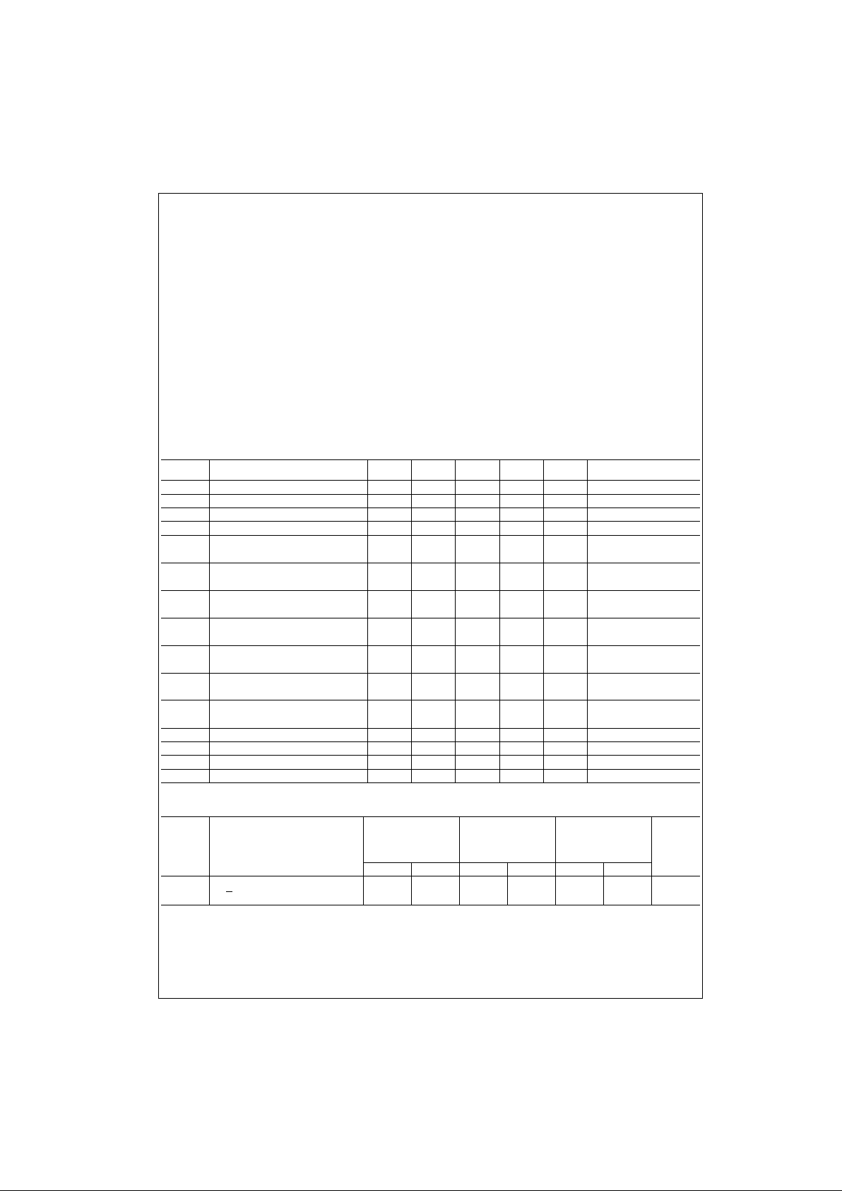
Absolute Maximum Ratings(Note 1) Recommended Operating
Conditions
Note 1: Absolute maximum ratings are values beyond which the device
may be damaged or have its useful life impaired. Functional operation
under these conditions is not implied.
Note 2: Either voltage limit or curr ent limit is sufficient to protect inputs.
DC Electrical Characteristics
AC Electrical Characteristics
Storage Temperature −65°C to +150°C
Ambient Temperature under Bias −55°C to +125°C
Junction Temperature under Bias −55°C to +175°C
V
CC
Pin Potential to Ground Pin −0.5V to +7.0V
Input Voltage (Note 2) −0.5V to +7.0V
Input Current (Note 2) −30 mA to +5.0 mA
Voltage Applied to Output
in HIGH State (with V
CC
= 0V)
Standard Output −0.5V to V
CC
3-STATE Output −0.5V to +5.5V
Current Applied to Output
in LOW State (Max) twice the rated I
OL
(mA)
ESD Last Passing Voltage (Min) 4000V
Free Air Ambient Temperature 0°C to +70°C
Supply Voltage +4.5V to +5.5V
Symbol Parameter Min Typ Max Units
V
CC
Conditions
V
T+
Positive-Going Threshold 1.5 1.7 2.0 V 5.0V
V
T−
Negative-Going Threshold 0.7 0.9 1.1 V 5.0V
∆V
T
Hysteresis (VT+–VT−) 0.4 0.8 V 5.0V
V
CD
Input Clamp Diode Voltage −1.2 V Min IIN = −18 mA
V
OH
Output HIGH 10% V
CC
2.5
VMin
IOH = −1 mA
Voltage 5% V
CC
2.7 IOH = −1 mA
V
OL
Output LOW 10% V
CC
0.5 V Min IOL = 20 mA
Voltage
I
IH
Input HIGH
5.0 µAMaxVIN = 2.7V
Current
I
BVI
Input HIGH Current
7.0 µAMaxVIN = 7.0V
Breakdown Test
I
CEX
Output HIGH
50 µAMaxV
OUT
= V
CC
Leakage Current
V
ID
Input Leakage
4.75 V Max
IID = 1.9 µA
Test All Other Pins Grounded
I
OD
Output Leakage
3.75 µA0.0
V
IOD
= 150 mV
Circuit Current All Other Pins Grounded
I
IL
Input LOW Current −0.6 mA Max VIN = 0.5V
I
OS
Output Short-Circuit Current −60 −150 mA Max V
OUT
= 0V
I
CCH
Power Supply Current 25 mA Max VO = HIGH
I
CCL
Power Supply Current 25 mA Max VO = LOW
Symbol Parameter
TA = +25°CT
A
= −55°C to +125°CTA = 0°C to +70°C
Units
VCC = +5.0V VCC = +5.0V VCC = +5.0V
CL = 50 pF CL = 50 pF CL = 50 pF
Min Max Min Max Min Max
t
PLH
Propagation Delay 4.0 10.5 4.0 13.0 4.0 11.5
ns
t
PHL
In→O
n
3.5 8.5 3.5 10.0 3.5 9.0
 Loading...