Fairchild Semiconductor 74F139SJX, 74F139SJ, 74F139SCX, 74F139SC, 74F139PC Datasheet
...
© 1999 Fairchild Semiconductor Corporation DS009479 www.fairchildsemi.com
April 1988
Revised July 1999
74F139 Dual 1-of-4 Decoder/Demultiplexer
74F139
Dual 1-of-4 Decoder/Demultiplexer
General Description
The F139 is a high-speed, dual 1-of-4 decoder/demultiplexer. The device has two independe nt decoders, each
accepting two inputs and provid ing four mutu ally exclus ive
active LOW outputs. Each decoder has an active LOW
Enable input which can be used as a data input for a 4-output demultiplexer. Each half of the F1 39 can be u sed as a
function generator pr oviding all four minte rms of two variables.
Features
■ Multifunction capability
■ Two completely independent 1-of-4 decoders
■ Active LOW mutually exclusive outputs
Ordering Code:
Devices also availab le in Tape and Reel. Specify by appending th e s uffix let t er “X” to the ordering code.
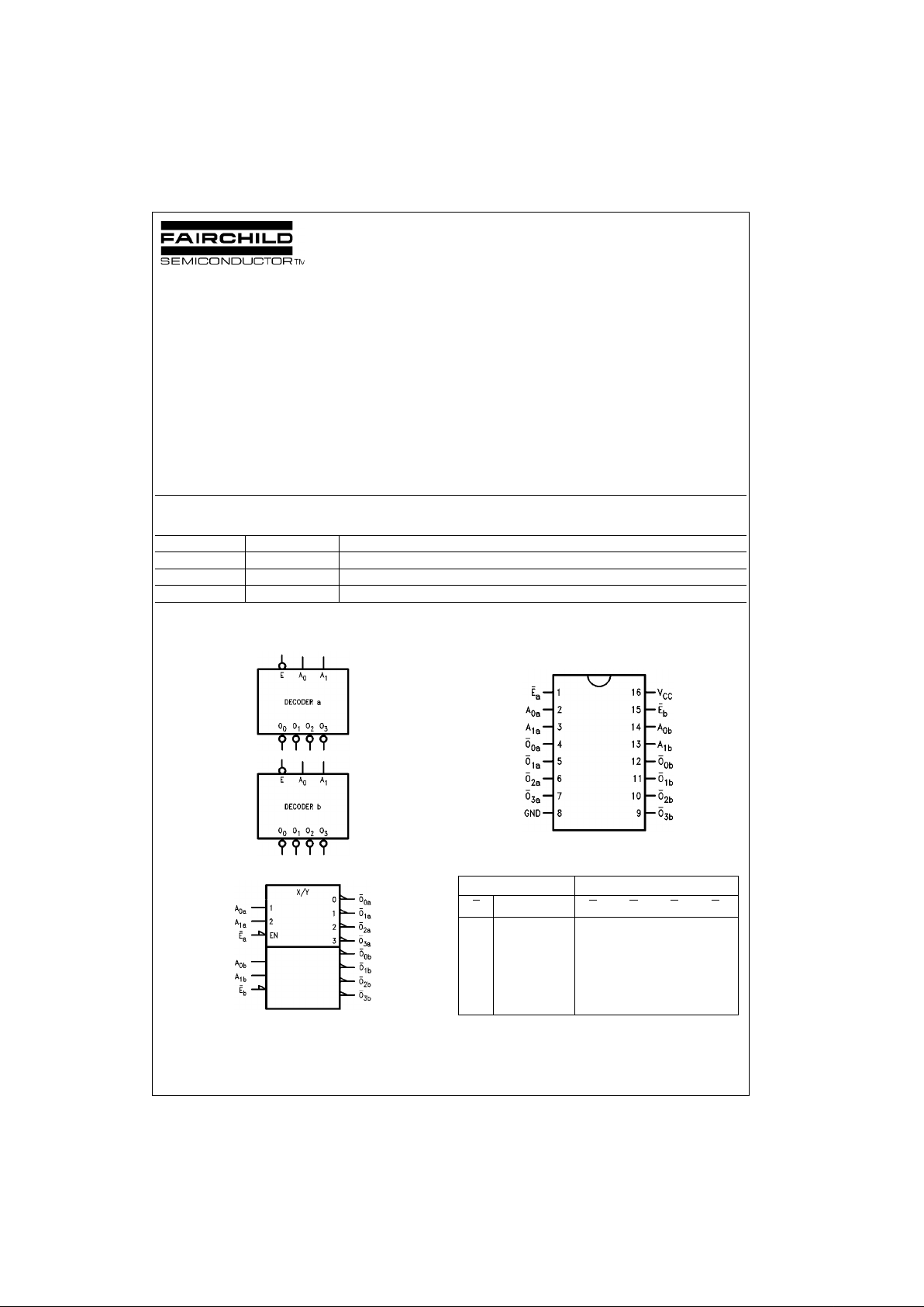
Logic Symbols
IEEE/IEC
Connection Diagram
Truth Table
H = HIGH Voltage Level
L = LOW Voltage Level
X = Immaterial
Order Number Package Number Package Description
74F139SC M16A 16-Lead Small Outline Integrated Circuit (SOIC), JEDEC MS-012, 0.150 Narrow
74F139SJ M16D 16-Lead Small Outline Package (SOP), EIAJ TYPE II, 5.3mm Wide
74F139PC N16E 16-Lead Plastic Dual-In-Line Package (PDIP), JEDEC MS-001, 0.300 Wide
Inputs Outputs
E
A
0
A
1
O
0
O
1
O
2
O
3
HXXHHHH
LLLLHHH
LHLHLHH
LLHHHLH
LHHHHHL

www.fairchildsemi.com 2
74F139
Unit Loading/Fan Out
Functional Description
The F139 is a high-speed dual 1-of-4 decoder/demultiplexer. The device has two independent deco ders, eac h of
which accepts two binary weighted inputs (A
0–A1
) and pro-
vides four mutually exclusive active LOW Outputs (O
0–O3
).
Each decoder has an active LOW enable (E
). When E is
HIGH all outp ut s ar e f or c ed HIG H. Th e en a bl e ca n be u s ed
as the data input for a 4-output de multiplexer applicatio n.
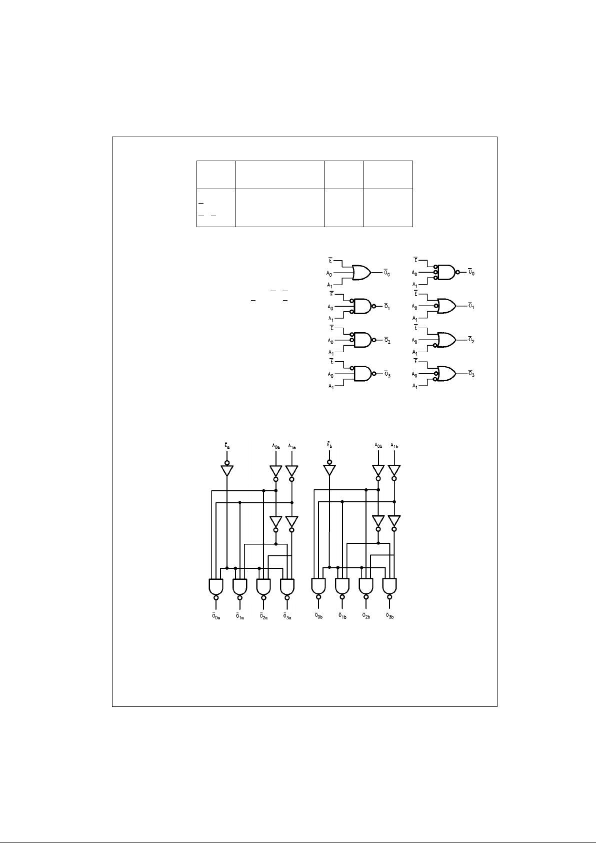
Each half of the F139 generates all four minterms of two
variables. These four minte rm s are use f ul in so me a ppl ica tions, replacing multiple gate functions as shown in
Figure 1, and thereby reducing the number of packages
required in a logic network.
FIGURE 1. Gate Functions (each half)
Logic Diagram
Please note that this diagram is provided o nly f or t he understanding of lo gic operations and should not be used to estimate propagation delays.
Pin Names Description
U.L.
Input I
IH/IIL
HIGH/LOW
Output I
OH/IOL
A0, A
1
Address Inputs 1.0/1.0 20 µA/−0.6 mA
E
Enable Inputs (Active LOW) 1.0/1.0 20 µA/−0.6 mA
O
0–O3
Outputs (Active LOW) 50/33.3 −1 mA/20 mA
 Loading...