

Fairchild Semiconductor 74F1056SCX Datasheet
© 1999 Fairchild Semiconductor Corporation DS011655 www.fairchildsemi.com
December 1993
Revised August 1999
74F1056 8-Bit Schottky Barrier Diode Array
74F1056
8-Bit Schottky Barrier Diode Array
General Description
The 74F1056 is an 8-bit Schottky barrier diode array
designed to be employed as termination on the inputs to
memory bus lines or CLOCK lines. This device is designed
to suppress negative transien ts caused by line re flections,
switching noise and crosstalk.
Features
■ 8-Bit array structure designed to suppress negative
transients
■ Guarante ed ESD protection (HBM) in excess of 4 kV
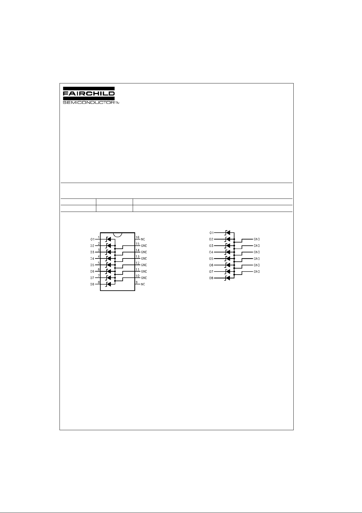
■ Common anode shared by all eight diodes
■ Broadside pinout for ease of bus routing
Ordering Code:
Devices also availab le in Tape and Reel. Specify by appending th e s uffix let t er “X” to the ordering cod e.
Connection Diagram Schematic Diagram
Order Number Package Number Package Description
74F1056SC M16A 16-Lead Small Outline Integrated Circuit (SOIC), JEDEC MS-012, 0.150 Narrow
www.fairchildsemi.com 2
74F1056
Absolute Maximum Ratings(Note 1)
Note 1: Absolute maximum rating s are valued beyond which the device
may be damaged or have its useful life impaired. Functional operation
under these conditi ons is not implied.
Note 2: These values apply for the t
w
≤ 100 µs, duty cycle ≤ 20%.
DC Electrical Characteristics
Over recommended operating free air temperature range, unless otherwise noted
SINGLE DIODE OPERATION (Note 3)
Note 3: These tests apply to separate diode operation, diodes not under test are open-circuit.
MULTIPLE DIODE OPERATION
Note 4: ICR is measured under the fo llowing conditions: One diode static, all ot hers switching
Switching diodes : t
W
= 100 µs; Static diode: VIN = 6V
Duty cycle = 20%, I
f
= 200 mA
The static diode input current is the internal crosstalk current I
CR
.
AC Electrical Characteristics
TA = 25°C
Storage Temperature −65°C to +150°C
Operating Free-Air Temperature 0°C to 70°C
Steady State Reverse Voltage, (V
R
)7.0V
Continuous Total Power Dissipation at or below
25°C Free-Air Temperature, (P
D
) 750 mW
Continuous Forward Current, (I
f
)
Any Output Pin to GND 50 mA
Total Through All GND Pins 170 mA
Repetitive Peak Forward Current, lfp (Note 2)
Any Output Pin to GND 300 mA
Total Through All GND Pins 1.2A
ESD (HBM) 4 kV
Symbol Parameter Min Typ Max Units Conditions
V
BR
Reverse Breakdown Voltage 7.0 V IR = 10 µA
I
R
Static Reverse Current 10 µAVR = 7V
V
F
Static Forward Voltage −0.65 −0.85 V IF = −16 mA
−0.8 −1.0 IF = −50 mA
C
T
Total Capacitance 5 10 pF VI = 0V, f = 1 MHz
48 V
I
= 2V, f = 1 MHz
Symbol Parameter Min Typ Max Units Conditions
I
CR
Internal Crosstalk Current 0.2 2 mA Total GND current = 1.2A (Note 4)
Symbol Parameter Min Typ Max Units Conditions
Figure
Number
V
FR
Forward Recovery Voltage 1.25 V IF = 300 mA Figure 1
T
RR
Reverse Recovery Time 5.0 ns IF = 10 mA, IR = 1 mA Figure 2
RL = 100Ω
 Loading...