

Fairchild Semiconductor 74ALVCH162240 Datasheet
November 2001
Revised November 2001
74ALVCH162240
Low Voltage 16-Bit Inverting Buffer/Line Driver
with Bushold and 26
Ω Series Resistors in Outputs
74ALVCH162240 Low Voltage 16-Bit Inverting Buffer/Line Driver
General Description
The ALVCH162240 contains sixteen invert ing buffers with
3-STATE outputs to be employed as a memory and
address driver, clock driver, or bus oriented transmitter/
receiver. The device is nibble (4-bit) controlled. Each nibble
has separate 3-STATE control inputs which can be shorted
together for full 16-bit operation.
The ALVCH162240 data inputs incl ude active b ushold circuitry, eliminating the need for external pull-up resistors to
hold unused or floating data inputs at a valid logic level.
The 74ALVCH162240 is also designed with 26
resistors in the outputs. This design reduces l ine noise in
applications such as memory address drivers, cl ock drivers, and bus transceivers/transmitters.
The 74ALVCH162240 is designed for low voltage (1.65V to
3.6V) V
The 74ALVCH162240 is fabricated with an advanced
CMOS technology to achieve high speed operation while
maintaining low CMOS power dissipation.
applications with output capability up to 3.6V.
CC
Ω series
Features
■ 1.65V to 3.6V VCC supply operation
■ 3.6V tolerant control inputs and outputs
■ Bushold on data inputs elimin atin g the nee d for exte rnal
pull-up/pull-down resistors
■ 26
Ω series resistors in outputs
■ t
PD
3.8 ns max for 3.0V to 3.6V V
4.3 ns max for 2.3V to 2.7V VCC
7.6 ns max for 1.65V to 1.95V V
■ Uses patented noise/EMI reductio n circuitr y
■ Latchup conforms to JEDEC JED78
■ ESD performance:
Human body model
Machine model
> 200V
CC
CC
> 2000V
Ordering Code:
Order Number Package Number Package Descriptions
74ALVCH162240T MTD48 48-Lead Thin Shrink Small Outline Package (TSSOP), JEDEC MO-153, 6.1mm Wide
Devices also availab le in Tape and Reel. Specify by appending the suffix letter “X” to the o rdering code.
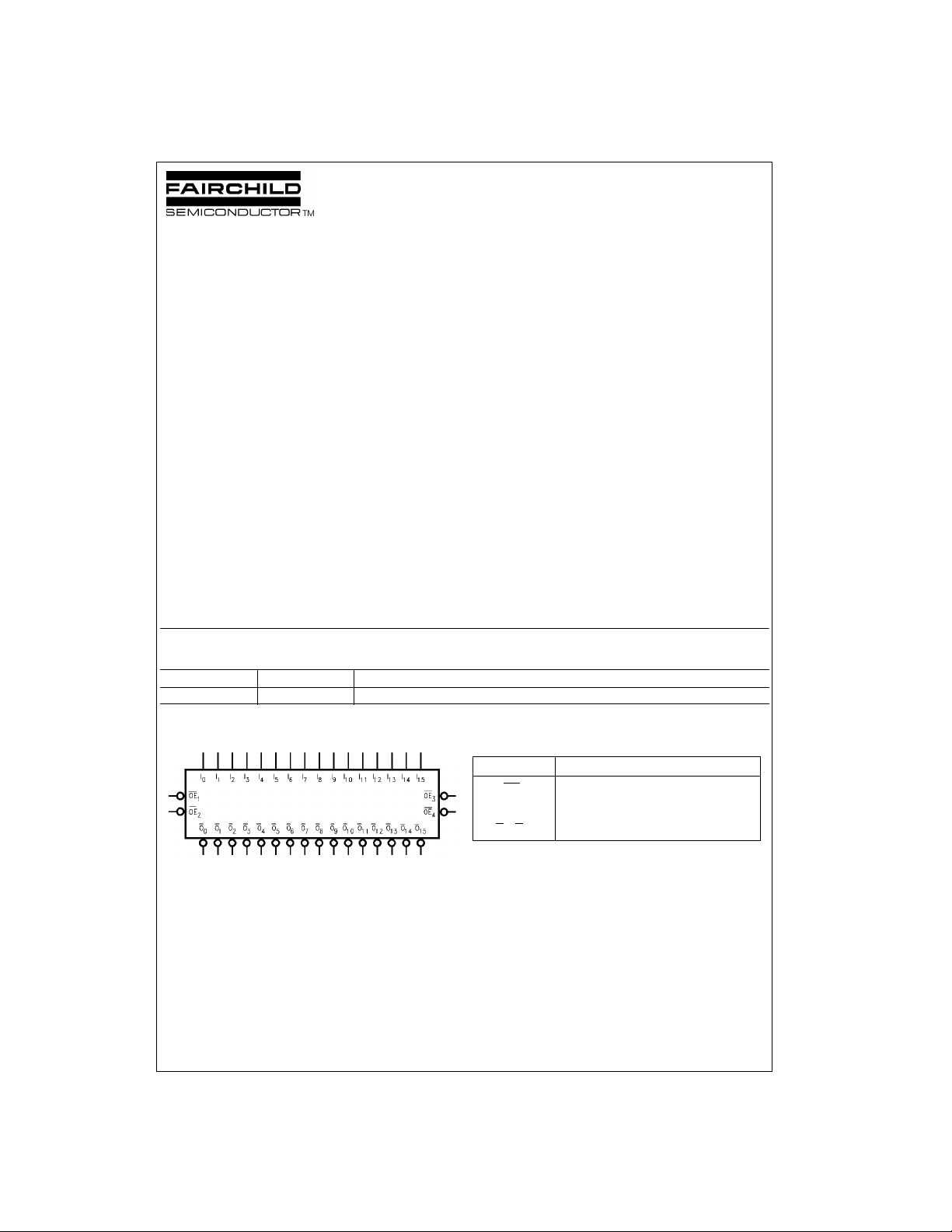
Logic Symbol Pin Descriptions
Pin Names Description
I
O
OE
n
0–I15
0–O15
Output Enable Input (Active LOW)
Bushold Inputs
Outputs
© 2001 Fairchild Semiconductor Corporation DS500700 www.fairchildsemi.com
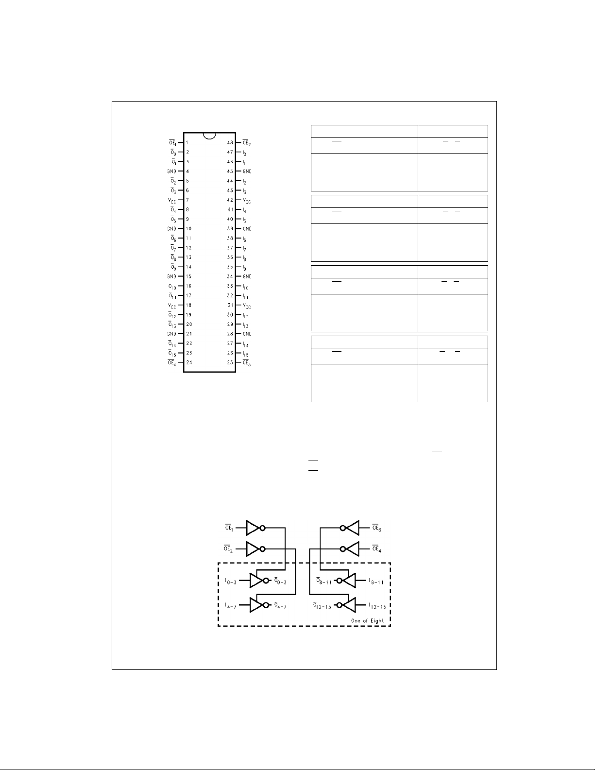
Connection Diagram Truth Tables
OE
LL H
LH L
74ALVCH162240
HX Z
OE
LL H
LH L
HX Z
OE
LL H
LH L
HX Z
OE
LL H
LH L
HX Z
H = HIGH Voltage Level
L = LOW Voltage Level
X = Immaterial (HIGH or LOW, inputs may not float)
Z = High Impedance
Inputs Outputs
1
I0–I
3
Inputs Outputs
2
I4–I
7
Inputs Outputs
3
I8–I
11
Inputs Outputs
4
I12–I
15
O0–O
O4–O
O8–O
O12–O
3
7
11
15
Functional Description
The 74ALVCH162240 contains sixteen inverting buffers
with 3-STATE outputs. The device is nibble (4 bits) controlled with each nibbl e fun ctioning identically, but independent of each other. The control pins may be shorted
together to obtain full 16- bit operation.The 3-STATE out-
Logic Diagram
www.fairchildsemi.com 2
puts are controlled by an Output Enable (OE
is LOW, the outputs are in the 2-state mode. When
OE
n
OE
is HIGH, the standard outputs ar e in the high imped-
n
) input. When
n
ance mode but this does not interfere with entering new
data into the inputs.
 Loading...