

Fairchild Semiconductor 74ALVCF322835 Datasheet
74ALVCF322835
Low Voltage 36-Bit Universal Bus Driver
with 3.6V Tolerant Outputs
and 26
Ω Series Resistors in Outputs
May 2002
Revised May 2002
74AL VCF322 835 Low Voltage 36-Bit Universal Bus Driver with 3.6V Tolerant Outputs and 26
Outputs
General Description
The 74ALVCF322835 low voltage 36-bit universal bus
driver combines D-type latches and D-type flip-flops to
allow data flow in transparent, latched and clocked modes.
Data flow is controll ed b y ou tpu t-enable (OE
(LE), and clock (CLK) inputs. The device operates in
Transparent Mode when LE is held HIGH. The device
operates in clocked mode when LE is LOW and CLK is toggled. Data transfer s f rom the In pu ts (I
a Positive Edge Transition of the Clock. When OE
the output data is enabl ed. When OE
port is in a high impedance state.
The 74ALVCF322835 is designed with 26
in the outputs. This d esign reduces noise in applic ations
such as memory address driver s, clock drivers, and bus
transceivers/transmitters.
The 74ALVCF322835 is designed for low voltage (1.65V to
3.6V) V
The 74ALVCF322835 is fabricated with an advanced
CMOS technology to achieve high speed operation while
maintaining low CMOS power dissipation.
applications with I/O capability up to 3.6V.
CC
), latch-enable
) to Outputs (On) on
n
is HIGH the output
is LOW,
Ω series resistors
Features
■ Compatible with PC133 DIMM module specifications
■ 1.65V to 3.6V V
■ 3.6V tolerant outputs
Ω series resistors in outputs
■ 26
■ t
(CLK to On)
PD
3.7 ns max for 3.0V to 3.6V V
4.6 ns max for 2.3V to 2.7V V
7.4 ns max for 1.65V to 1.95V V
■ Power-down high impedance outputs
■ Latchup conforms to JEDEC JED78
■ ESD performance:
Human body model
Machine model
CC
Ordering Code:
Order Number
74ALVCF322835G
(Note 1) (Note 2)
Note 1: Ordering Code “G” indicates Trays.
Note 2: Devices also available in Tape and Reel. Specify by appending th e s uffix let t er “X” to the ordering code.
Package
Number
BGA114A 114-Ball Fine-Pitch Ball Grid Array (FBGA), JEDEC MO-205, 5.5mm Wide
Package Description
specifications provided
CC
CC
CC
> 2000V
>200V
© 2002 Fairchild Semiconductor Corporation DS500741 www.fairchildsemi.com
Ω
Series Resistors in
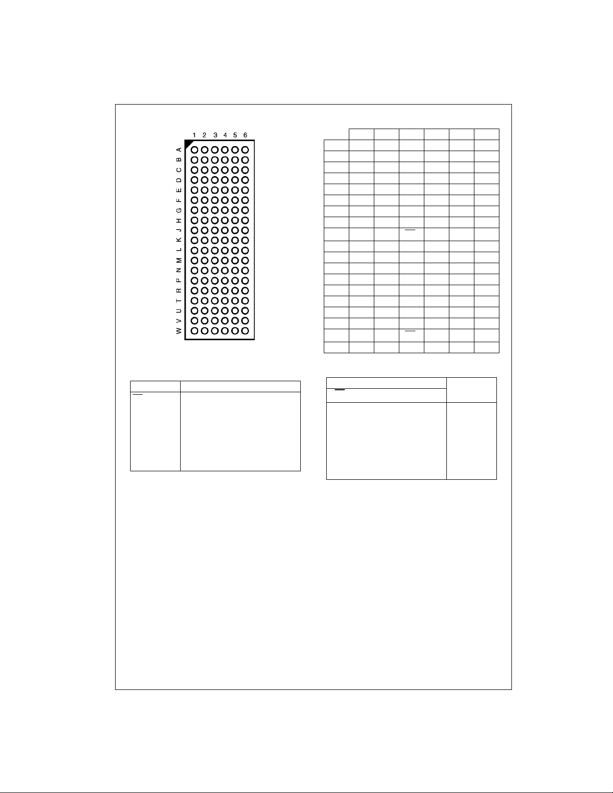
Connection Diagram
74ALVCF322835
(Top Thru View)
Pin Descriptions
Pin Names Description
OE
LE
CLK
1I
2I
1O
2O
1
1
n
n
- 1I
- 2I
1
1
n
- 1O
- 2O
Output Enable Input (Active LOW)
Latch Enable Input
Clock Input
Data Inputs
18
Data Inputs
18
3-STATE Outputs
18
3-STATE Outputs
18
FBGA Pin Assignments
123456
A 1O
B 1O41O3NC GND 1I31I
C 1O61O5GND GND 1I51I
D 1O81O7V
E 1O101O9GND GND 1I91I
F 1I121O11GND GND 1I111I
G 1O141O13V
H 1O151O16GND GND 1I161I
J 1O171O18OE1CLK11I181I
1O1NC NC 1I11I
2
CCVCC1I7
CCVCC1I131I14
2
4
6
1I
8
10
12
15
17
K NC NC LE1GND NC NC
L 2O
M 2O42O3GND GND 2I32I
N 2O62O5V
P 2O82O7GND GND 2O72I
R 2O102O9GND GND 2I92I
T 2O122O11V
U 2O142O13GND GND 2I132I
V 2O152O16OE2CLK22I162I
W 2O172O18LE2GND 2I182I
2O1NC GND 2I12I
2
CCVCC2I5
CCVCC2I112I12
2
4
2I
6
8
10
14
15
17
Truth Table
Inputs Outputs
OE
H = Logic HIGH
L = Logic LOW
X = Don’t Care, but not floating
Z = High Impedance
↑ = LOW-to-HIGH Clock Transition
Note 3: Output level be fore the indicated steady-s tate input conditions
were established provided that CLK wa s HIGH before LE went L OW.
Note 4: Output level be fore the indicated steady-s tate input conditions
were established.
n
LEnCLK
I
n
n
O
n
HXXX Z
LHXL L
LHXH H
LL
LL
LLHXO
LLLXO
↑ LL
↑ HH
(Note 3)
0
(Note 4)
0
www.fairchildsemi.com 2
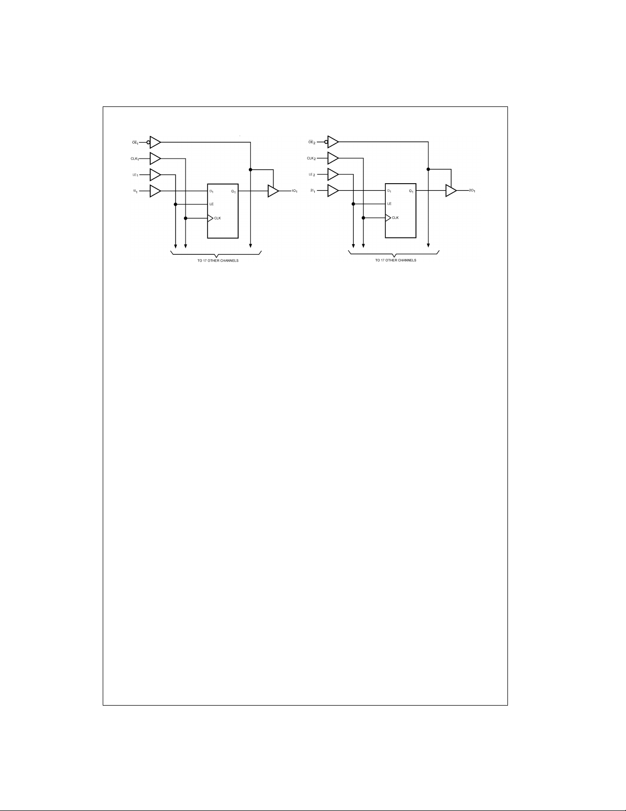
Logic Diagram
74ALVCF322835
3 www.fairchildsemi.com
 Loading...