

Fairchild Semiconductor 74ALVCF162835 Datasheet
September 2001
Revised October 2001
74ALVCF162835
Low Voltage 18-Bit Universal Bus Driver with 3.6V
Tolerant Outputs and 26
Ω Series Resistors in Outputs
74AL VCF162 835 Low Voltage 18-Bit Uni versal Bus Driver with 3.6V Tole rant Outputs and 26
Outputs
General Description
The 74ALVCF162835 low voltage 18-bit universal bus
driver combines D-type latches and D-type flip-flops to
allow data flow in transparent, latched and clocked modes.
Data flow is controll ed b y ou tpu t-enable (OE
(LE), and clock (CLK) inputs. The device operates in
Transparent Mode when LE is held HIGH. The device
operates in clocked mode when LE is LOW and CLK is toggled. Data transfer s f rom the In pu ts (I
a Positive Edge Transition of the Clock. When OE
the output data is enabl ed. When OE
port is in a high impedance state.
The 74ALVCF162835 is designed with 26
in the outputs. This d esign reduces noise in applic ations
such as memory address driver s, clock drivers, and bus
transceivers/transmitters.
The 74ALVCF162835 is designed for low voltage (1.65V to
3.6V) V
The 74ALVCF162835 is fabricated with an advanced
CMOS technology to achieve high speed operation while
maintaining low CMOS power dissipation.
applications with I/O capability up to 3.6V.
CC
), latch-enable
) to Outputs (On) on
n
is HIGH the output
is LOW,
Ω series resistors
Features
■ Compatible with PC133 DIMM module specifications
■ 1.65V-3.6V V
■ 3.6V tolerant outputs
■ 26
Ω series resistors in outputs
■ t
(CLK to On)
PD
3.7 ns max for 3.0V to 3.6V V
4.6 ns max for 2.3V to 2.7V V
7.4 ns max for 1.65V to 1.95V V
■ Power-down high impedance outputs
■ Latchup conforms to JEDEC JED78
■ ESD performance:
Human body model
Machine model
specifications provided
CC
> 2000V
>200V
CC
CC
CC
Ordering Code:
Order Number
74ALVCF162835T MTD56 56-Lead Thin Shrink Small Outline Package (TSSOP), JEDEC MO-153, 6.1mm Wide
Devices also availab le in Tape and Reel. Specify by appending the suffix letter “X” to the o rdering code.
Package
Number
Package Description
© 2001 Fairchild Semiconductor Corporation DS500668 www.fairchildsemi.com
Ω
Series Resistors in
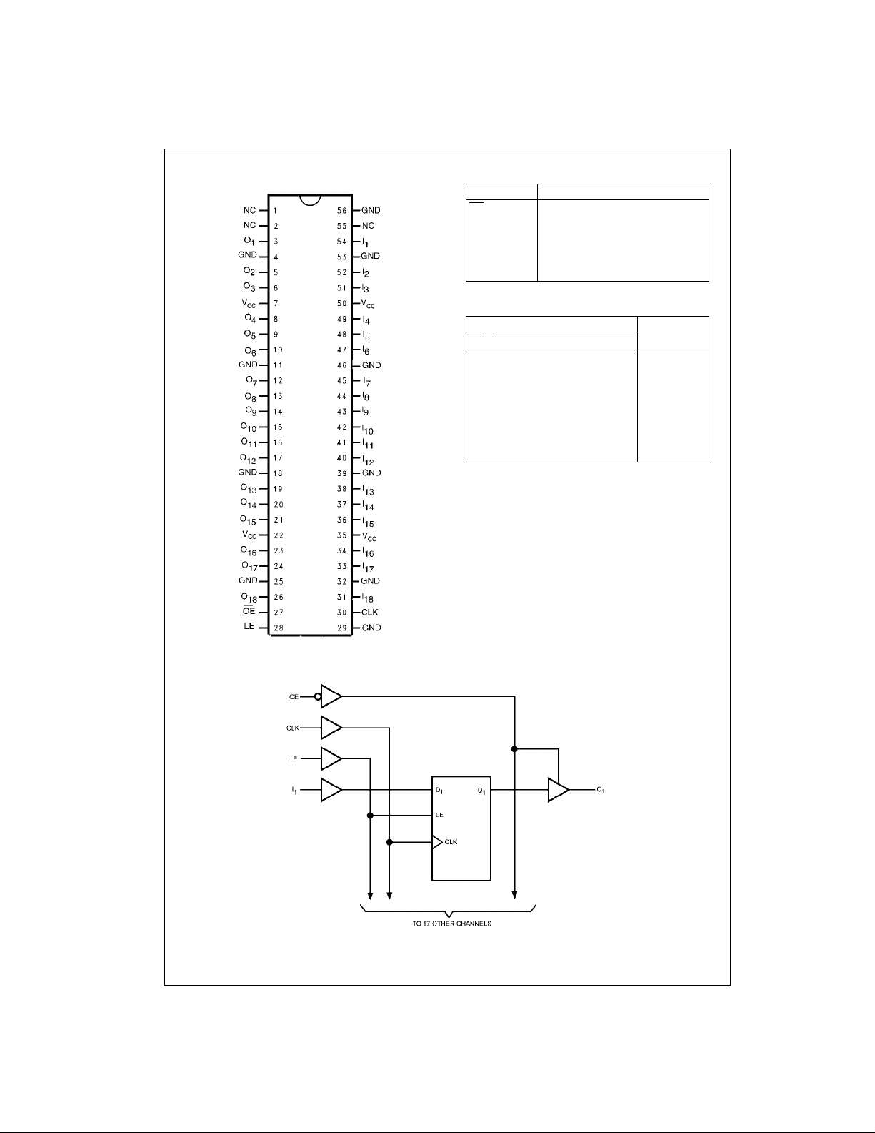
Connection Diagram Pin Descriptions
Pin Names Descriptio n
OE
LE Latch Enable Input
CLK Clock Input
I
- I
1
74ALVCF162835
18
- O
O
1
18
Truth Table
OE
H = Logic HIGH
L = Logic LOW
X = Don’t Care, but not floating
Z = High Impedance
↑ = LOW-to-HIGH Clock Transition
Note 1: Output level be fore the indicated steady-s tate input conditions
were established provided that CLK wa s HIGH before LE went L OW.
Note 2: Output level be fore the indicated steady-s tate input conditions
were established.
LE CLK
HXXX Z
LHXL L
LHXH H
LL
LL
LLHXO
LLLXO
Output Enable Input (Active LOW)
Data Inputs
3-STATE Outputs
Inputs Outputs
I
n
O
n
↑ LL
↑ HH
(Note 1)
0
(Note 2)
0
Logic Diagram
www.fairchildsemi.com 2
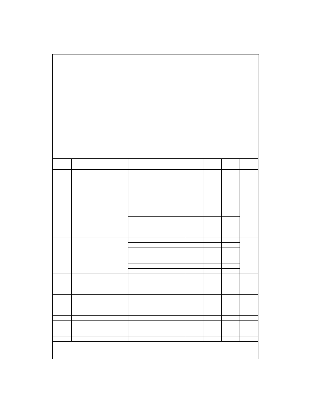
Absolute Maximum Ratings(Note 3) Recommended Operating
Supply Voltage (VCC) −0.5V to +4.6V
DC Input Voltage (V
Output Voltage (V
DC Input Diode Current (I
V
< 0V −50 mA
I
DC Output Diode Current (I
< 0V −50 mA
V
O
) −0.5V to 4.6V
I
) (Note 4) −0.5V to VCC +0.5V
O
)
IK
)
OK
DC Output Source/Sink Current
(I
) ±50 mA
OH/IOL
or GND Current per
DC V
CC
Supply Pin (I
Storage Temperature Range (T
or GND) ±100 mA
CC
) −65°C to +150°C
STG
Conditions
Power Supply
Operating 1.65V to 3.6V
Input Voltage 0V to V
Output Voltage (VO)0V to V
Free Air Operating Temperature (TA) −40°C to +85°C
Minimum Input Edge Rate (
= 0.8V to 2.0V, VCC = 3.0V 10 ns/V
V
IN
Note 3: The Absolute Maxi mum Ratings are thos e values beyond which
the safety of the d evice cannot b e guaranteed . The device sh ould not be
operated at these limit s. The parametric values defi ned in the Electrical
Characteristics tables are not guaranteed at the Absolute Maximum Ratings. The “Recommended Operating Conditions” table will define the conditions for actual device oper ation.
Absolute Maximum Rating must be observed.
Note 4: I
O
Note 5: Floating or unused control inputs must be held HIGH or LOW.
(Note 5)
∆t/∆V)
DC Electrical Characteristics
V
Symbol Parameter Conditions
V
IH
V
IL
V
OH
V
OL
I
OH
I
OL
I
I
I
OZ
I
OFF
I
CC
∆I
HIGH Level Input Voltage 1.65 - 1.95 0.65 x V
LOW Level Input Voltage 1.65 - 1.95 0.35 x V
HIGH Level Output Voltage IOH = −100 µA 1.65 - 3.6 VCC - 0.2
LOW Level Output Voltage IOL = 100 µA 1.65 - 3.6 0.2
High Level Output Current 1.65 −2
Low Level Output Current 1.65 2
Input Leakage Current 0 ≤ VI ≤ 3.6V 1.65 - 3.6 ±5.0 µA
3-STATE Output Leakage 0 ≤ VO ≤ 3.6V, VI = VIH or V
Power Off Leakage Current 0V ≤ (VI, VO) ≤ 3.6V 0 10 mA
Quiescent Supply Current VI = VCC or GND, IO = 0 3.6 40 µA
Increase in ICC per Input VIH = VCC − 0.6V 2.7 - 3.6 750 µA
CC
IOH = −2 mA 1.65 1.2
I
= −4 mA 2.3 1.9
OH
= −6 mA 2.3 1.7
I
OH
I
= −8 mA 2.7 2
OH
= −12 mA 3.0 2
I
OH
I
= 2 mA 1.65 0.45
OL
= 4 mA 2.3 0.4
I
OL
IOL = 6 mA 2.3 0.55
IOL = 8 mA 2.7 0.6
IOL = 12 mA 3.0 0.8
IL
CC
(V)
2.7 - 3.6 2.0
2.7 - 3.6 0.8
3.0 2.4
3.0 0.55
2.3 −6
2.7 −8
3.0 −12
2.3 6
2.7 8
3.0 12
1.65 - 3.6 ± 10 µA
Min Max Units
CC
74ALVCF162835
CC
CC
V2.3 - 2.7 1.7
CC
V2.3 - 2.7 0.7
V
V
mA
mA
3 www.fairchildsemi.com
 Loading...