

Fairchild Semiconductor 74ALVC245 Datasheet
74ALVC245
Low Voltage Bidirectional Transceiver
with 3.6V Tolerant Inputs and Outputs
74ALVC245 Low Voltage Bidirectional Transceiver with 3.6V Tolerant Inputs and Outputs
September 2001
Revised February 2002
General Description
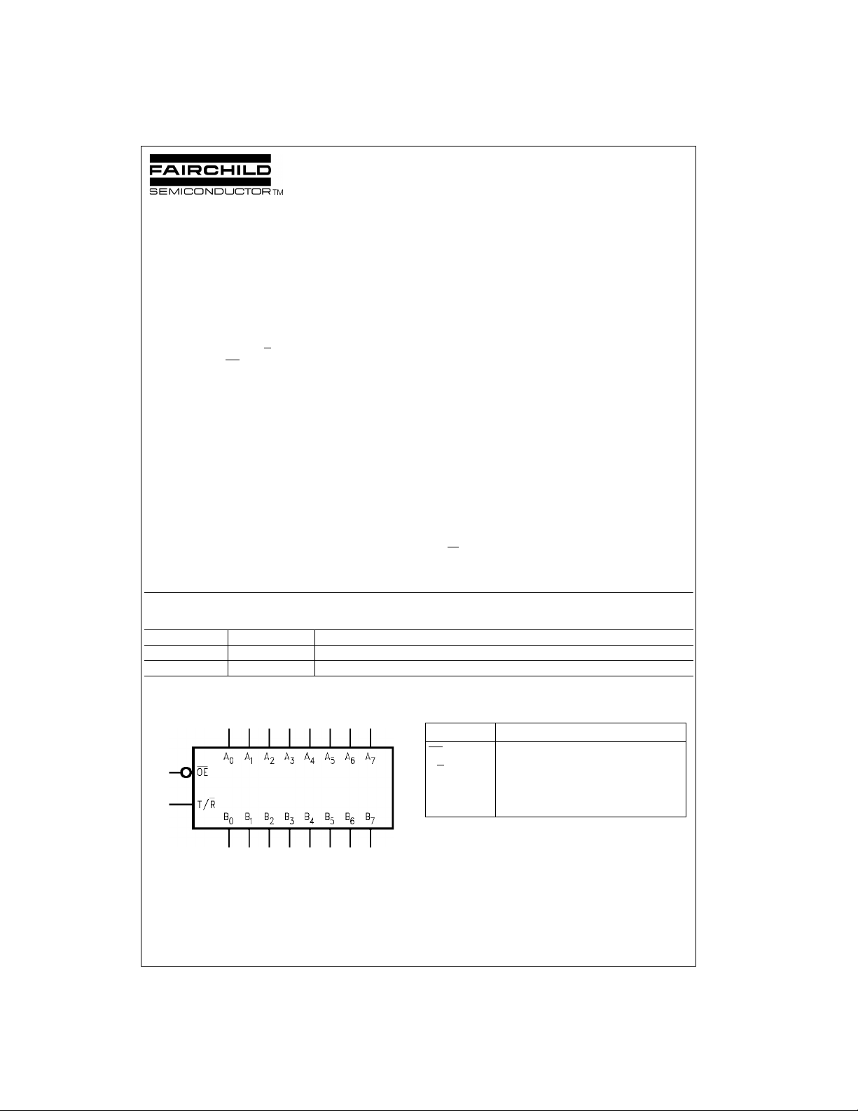
The ALVC245 contains eight non-inverting bidirectional
buffers with 3-STATE outputs and is in tended for bus oriented applications . The T/R
of data flow. The OE
by placing them in a high impedance state.
The 74ALVC245 is designed for low voltage (1.65V to
3.6V) V
The 74ALVC245 is fabricated with an advanced CMOS
technology to achieve high-speed operation while maintaining low CMOS power dissipation.
applications with I/O compatibility up to 3.6V.
CC
input determines the direction
input disables both th e A and B ports
Features
■ 1.65V to 3.6V VCC supply operation
■ 3.6V tolerant inputs and outputs
■ Power-off high impedance inputs and outputs
■ Supports Live Insertion and Withdrawal (Note 1)
■ t
PD
3.4 ns max for 3.0V to 3.6V V
3.9 ns max for 2.3V to 2.7V V
6 ns max for 1.65V to 1.95V V
■ Uses patented Quiet Series noise/EMI reduction
circuitry
■ Latchup conforms to JEDEC JED78
■ ESD performance:
Human body model
Machine model
Note 1: To ensure the high impedance state during power up and power
down, OE
should be tied to VCC through a pul l up res istor. The min imum
n
value of the resistor is dete rmined by the curren t sourcing capabilit y of the
driver.
> 200V
CC
CC
CC
> 2000V
Ordering Code:
Order Number Package Number Package Description
74ALVC245WM M20B 20-Lead Small Outline Integrated Circuit (SOIC), JEDEC MS-013, 0.300" Wide
74ALVC245MTC MTC20 20-Lead Thin Shrink Small Outline Package (TSSOP), JEDEC MO-153, 4.4mm Wide
Devices also availab le in Tape and Reel. Specify by appending the suffix letter “X” to the o rdering code.
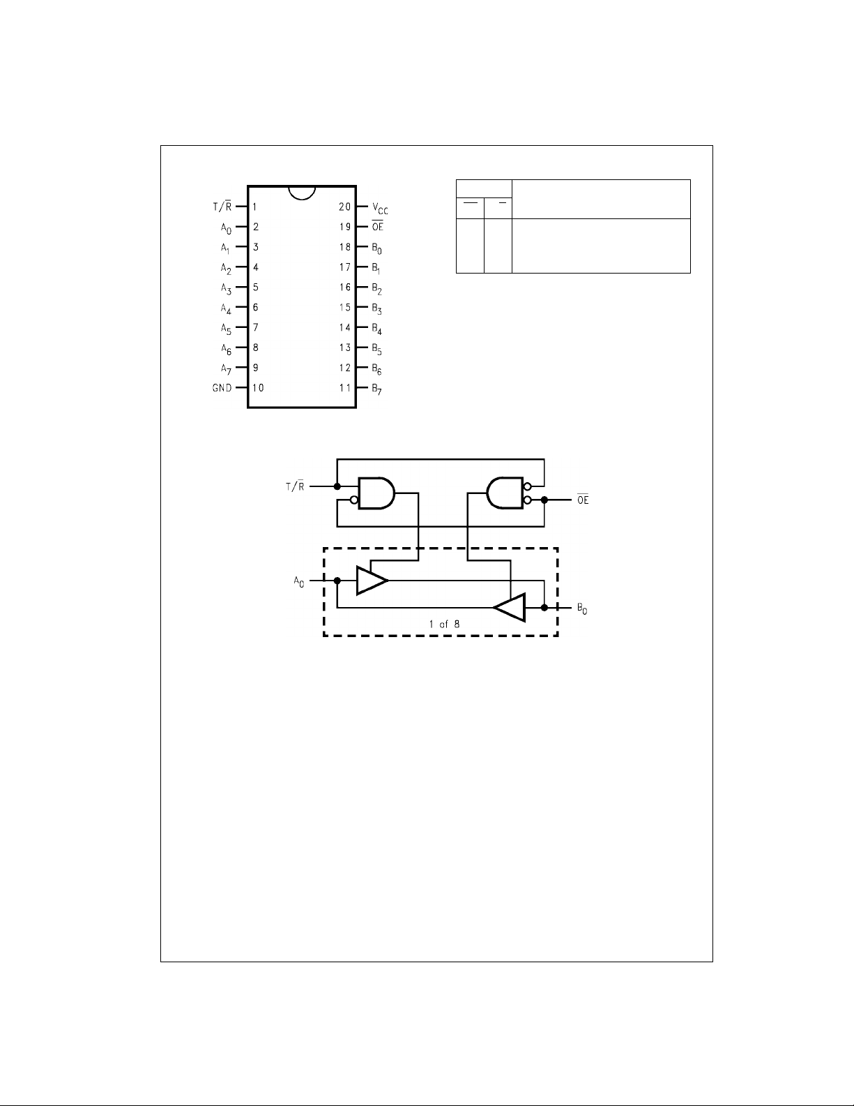
Logic Symbol Pin Descriptions
Pin Names Description
OE
T/R
A
0–A7
B
0–B7
Quiet Series is a tra demark of Fairchild Semiconductor Corp oration.
© 2002 Fairchild Semiconductor Corporation DS500647 www.fairchildsemi.com
Output Enable Input (Active LOW)
Transmit/Receive Input
Side A Inputs or 3-STATE Outputs
Side B Inputs or 3-STATE Outputs
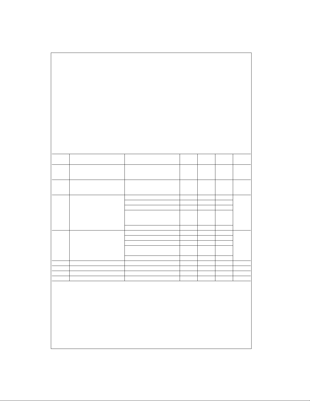
Connection Diagram Truth Table
Inputs Outputs
OE
74ALVC245
LLBus B0–B7 Data to Bus A0–A
LHBus A0–A7 Data to Bus B0–B
H X HIGH Z State on A0–A7, B0–B7 (Note 2)
H = HIGH Voltage Level
L = LOW Voltage Level
X = Immaterial
Z = High Impedance
Note 2: Unused bus terminals during HIGH Z State must be held HIGH or
LOW.
Logic Diagram
T/R
7
7
www.fairchildsemi.com 2
Absolute Maximum Ratings(Note 3) Recommended Operating
Supply Voltage (VCC) −0.5V to +4.6V
DC Input Voltage (V
Output Voltage (V
DC Input Diode Current (I
V
< 0V −50 mA
I
DC Output Diode Current (I
< 0V −50 mA
V
O
) −0.5V to 4.6V
I
) (Note 4) −0.5V to VCC +0.5V
O
)
IK
)
OK
DC Output Source/Sink Current
(I
) ±50 mA
OH/IOL
or GND Current per
DC V
CC
Supply Pin (I
Storage Temperature Range (T
or GND) ±100 mA
CC
) −65°C to +150°C
STG
Conditions
Power Supply
Operating 1.65V to 3.6V
Input Voltage (V
Output Voltage (VO)0V to V
Free Air Operating Temperature (TA) −40°C to +85°C
Minimum Input Edge Rate (
= 0.8V to 2.0V, VCC = 3.0V 10 ns/V
V
IN
Note 3: The Absolute Maxi mum Ratings are thos e values beyond which
the safety of the d evice cannot b e guaranteed . The device sh ould not be
operated at these limit s. The parametric values defi ned in the Electrical
Characteristics tables are not guaranteed at the Absolute Maximum Ratings. The “Recommended Operating Conditions” table will define the conditions for actual device oper ation.
Absolute Maximum Rating must be observed, limited to 4.6V.
Note 4: I
O
Note 5: Floating or unused control inputs must be held HIGH or LOW.
(Note 5)
)0V to V
I
∆t/∆V)
DC Electrical Characteristics
V
Symbol Parameter Conditions
V
IH
V
IL
V
OH
V
OL
I
I
I
OZ
I
CC
∆I
CC
HIGH Level Input Voltage 1.65 - 1.95 0.65 x V
LOW Level Input Voltage 1.65 - 1.95 0.35 x V
HIGH Level Output Voltage IOH = −100 µA 1.65 - 3.6 VCC - 0.2
LOW Level Output Voltage IOL = 100 µA 1.65 - 3.6 0.2
Input Leakage Current 0 ≤ VI ≤ 3.6V 3.6 ±5.0 µA
3-STATE Output Leakage 0 ≤ VO ≤ 3.6V 3.6 ±10 µA
Quiescent Supply Current VI = VCC or GND, IO = 0 3.6 10 µA
Increase in ICC per Input VIH = VCC − 0.6V 3 - 3.6 750 µA
IOH = −4 mA 1.65 1.2
I
= −6 mA 2.3 2.0
OH
= −12 mA 2.3 1.7
I
OH
IOH = −24 mA 3.0 2
I
= 4 mA 1.65 0.45
OL
= 6 mA 2.3 0.4
I
OL
IOL = 12 mA 2.3 0.7
IOL = 24 mA 3.0 0.55
CC
(V)
2.7 - 3.6 2.0
2.7 - 3.6 0.8
2.7 2.2
3.0 2.4
2.7 0.4
Min Max Units
CC
74ALVC245
CC
CC
V2.3 - 2.7 1.7
CC
V2.3 - 2.7 0.7
V
V
3 www.fairchildsemi.com
 Loading...