

Fairchild Semiconductor 74ALVC16839 Datasheet
December 2001
Revised December 2001
74ALVC16839
Low Voltage 20-Bit Selectable Register /Buffer
with 3.6V Tolerant Inputs and Outputs
74ALVC16839 Low Voltage 20-Bit Selectable Register/Buffer with 3.6V Tolerant Inputs and Outputs
General Description
The ALVC16839 contains twenty non-inverting selectable
buffered or registered pa ths. T he dev ic e can be c onfi g ur ed
to operate in a regis tered, or flow throu gh buffer mode by
utilizing the register enable (REGE) and Clock (CLK) signals. The device operates in a 20-bit word wide mode. All
outputs can be placed into 3-STATE through use of the OE
pin. These devices ar e ideally sui ted for buffered or registered 168 pin and 200 pin SDRAM DIMM me mory modules.
The 74ALVC16839 is designed for low voltage (1.65V to
3.6V) V
The 74ALVC16839 is fabricated w ith an advanc ed CMOS
technology to achieve high speed operation while maintaining low CMOS power dissipation.
applications with I/O compatibility up to 3.6V.
CC
Features
■ Compatible with PC100 and PC133 DIMM module
specifications
■ 1.65V to 3.6V V
■ 3.6V tolerant inputs and outputs
■ t
(CLK to On)
PD
3.7 ns max for 3.0V to 3.6V V
4.9 ns max for 2.3V to 2.7V VCC
8.8 ns max for 1.65V to 1.95V V
■ Power-off high impedance inputs and outputs
■ Supports live insertion and withdrawal (Note 1)
■ Uses patented noise/EMI reductio n circuitr y
■ Latchup conforms to JEDEC JED78
■ ESD performance:
Human body model
Machine model
Note 1: To ensure the high-impedance state d uring power up or power
should be tied to VCC through a pull-up r esistor; the min imum
down, OE
value of the res istor is d eter mine d by the cu rre nt-sou rcin g ca pa bility of t he
driver.
supply operation
CC
> 2000V
> 200V
CC
CC
Ordering Code:
Order Number Package Number Package Descriptions
74ALVC16839MTD MTD56 56-Lead Thin Shrink Small Outline Package (TSSOP), JEDEC MO-153, 6.1mm Wide
Devices also availab l e in Tape and Reel. Specify by appending su ffix let te r “X” to the ordering code.
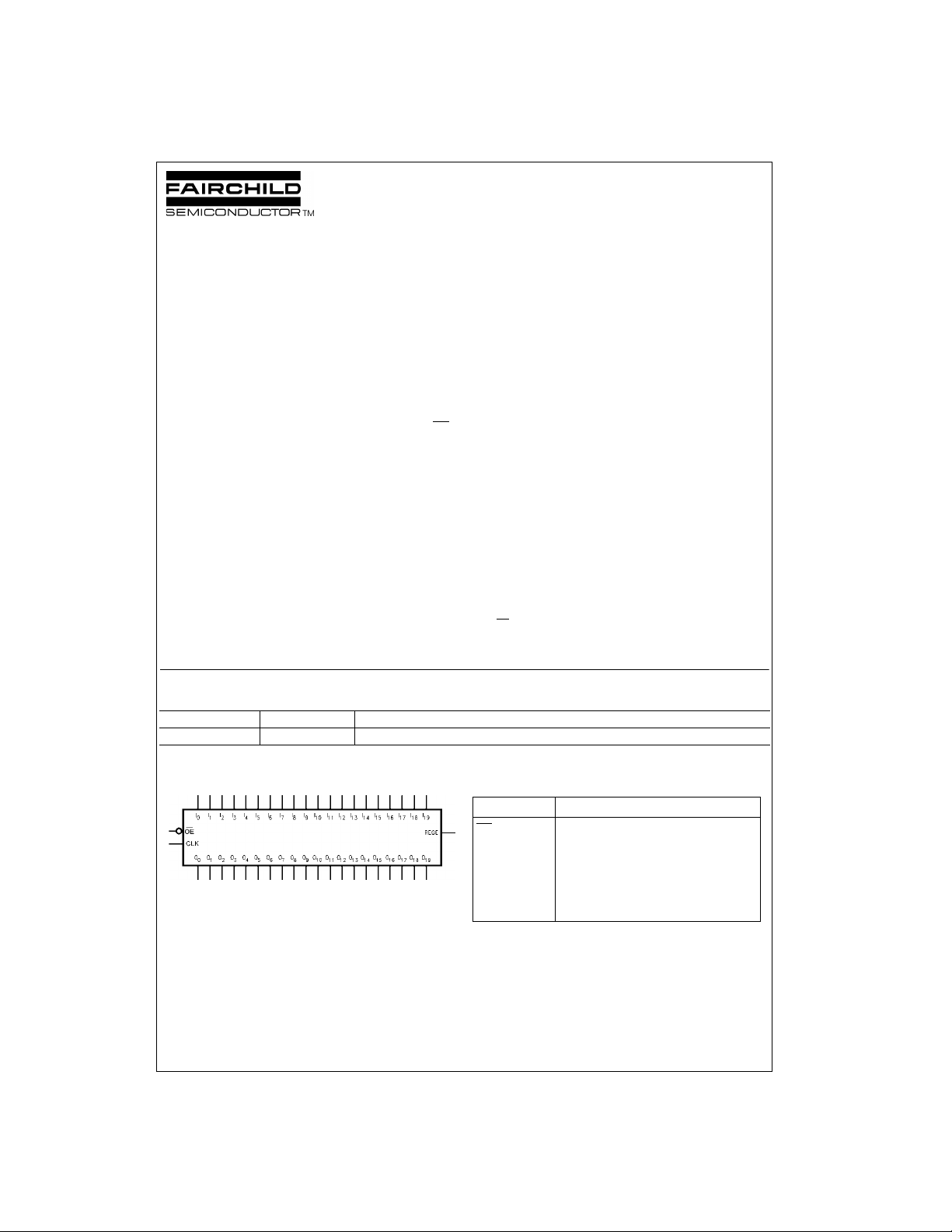
Logic Symbol Pin Descriptions
Pin Names Description
OE
I
0–I19
O
0–O19
CLK Clock Input
REGE Register Enable Input
© 2001 Fairchild Semiconductor Corporation DS500713 www.fairchildsemi.com
Output Enable Input (Active LOW)
Inputs
Outputs
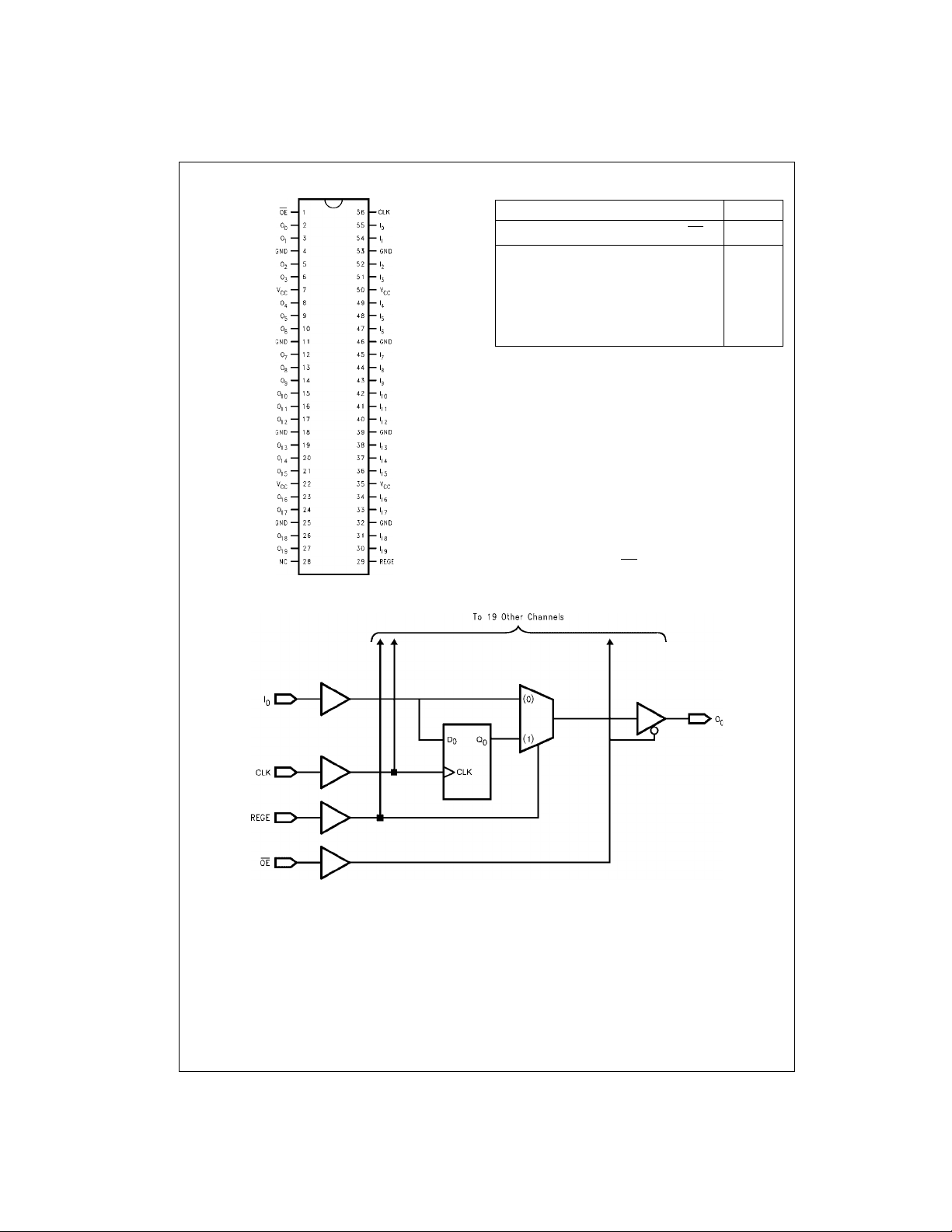
Connection Diagram Truth Table
CLK REGE
74ALVC16839
↑ HHL H
↑ HLL L
XLHLH
XLLLL
XXXHZ
H = Logic HIGH
L = Logic LOW
X = Don’t Care, but not floating
Z = High Impedance
↑ = LOW-to-HIGH Clock Transition
Functional Description
The 74ALVC16839 consists of twenty selectable noninverting buffers or regist ers with word wi de modes. Mode
functionality is selected through operation of the CLK and
REGE pin as shown by the truth table. When REGE is held
at a logic HIGH the device oper ates as a 20-bit register.
Data is transferred from I
CLK input. When the REG E pin i s held a t a l ogic LOW the
device operates in a flow through mode and data propagates directly from the I
be 3-stated by holding the OE
Logic Diagram
Inputs Outputs
I
n
to On on the rising edge of the
n
to the On outputs. All outputs can
n
pin at a logic HIGH.
OE
O
n
www.fairchildsemi.com 2
 Loading...