

Fairchild Semiconductor 74ALVC16501 Datasheet
October 2001
Revised October 2001
74ALVC16501
Low Voltage 18-Bit Universal Bus Transceivers
with 3.6V Tolerant Inputs and Outputs
74ALVC16501 Low Voltage 18-Bit Universal Bus Transceivers with 3.6V Tolerant Inputs and Outputs
General Description
The ALVC16501 is an 18-bit universal bus transceiver
which combines D-type latches and D-type flip-flops to
allow data flow in transparent, latched, and clocked modes.
Data flow in each dir ection is controlled by output-enable
(OEAB and OEBA
clock (CLKAB and CLKBA) inputs . F or A-to -B dat a f low, the
device operates in the transparent mode when LEAB is
HIGH. When LEAB is LOW, the A data is latched if CLKAB
is held at a HIGH or LOW logic level. If LEAB is LOW, the A
bus data is stored in the latch/flip-flop on the LOW-to-HIGH
transition of CLKAB. When OEAB is HIGH, the outputs are
active. When OEAB is LOW, the outputs are in a highimpedance state.
Data flow for B to A is similar to tha t of A to B but uses
OEBA
, LEBA, and CLKBA. The output enables are complementary (OEAB is active HIGH and OEBA
LOW).
The ALVC16501 is designed for low voltage (1.65V to
3.6V) V
CC
The ALVC16501 is fabricated with an advanced CMOS
technology to achieve high speed operation while maintaining low CMOS power dissipation.
), latch-enable (LEAB and LEBA), and
is active
applications with I/O capability up to 3.6V.
Features
■ 1.65V–3.6V VCC supply operation
■ 3.6V tolerant inputs and outputs
(A to B, B to A)
■ t
PD
3.4 ns max for 3.0V to 3.6V V
4.0 ns max for 2.3V to 2.7V V
7.0 ns max for 1.65V to 1.95V V
■ Power-down high impedance inputs and outputs
■ Supports live insertion/withdrawal (Note 1)
■ Uses patented noise/EMI reductio n circuitr y
■ Latchup conforms to JEDEC JED78
■ ESD performance:
Human body model
Machine model
Note 1: To ensure the high-impedance state d uring power up or power
down, OEBA
should be tied to G ND thro ugh a pull-dow n resist or; the m inimu m val ue of
the resistors is determined by the curren t- s ourcing capability of t he driver.
should be tied to VCC through a pull-up res istor and OEAB
>200V
CC
CC
CC
> 2000V
Ordering Code:
Order Number Package Number Package Description
74ALVC16501MTD MTD56 56-Lead Thin Shrink Small Outline Package (TSSOP), JEDEC MO-153, 6.1mm Wide
Devices also available on Tape and Reel. Specify by appending the suffix letter “X” to the ordering code.
© 2001 Fairchild Semiconductor Corporation DS500683 www.fairchildsemi.com
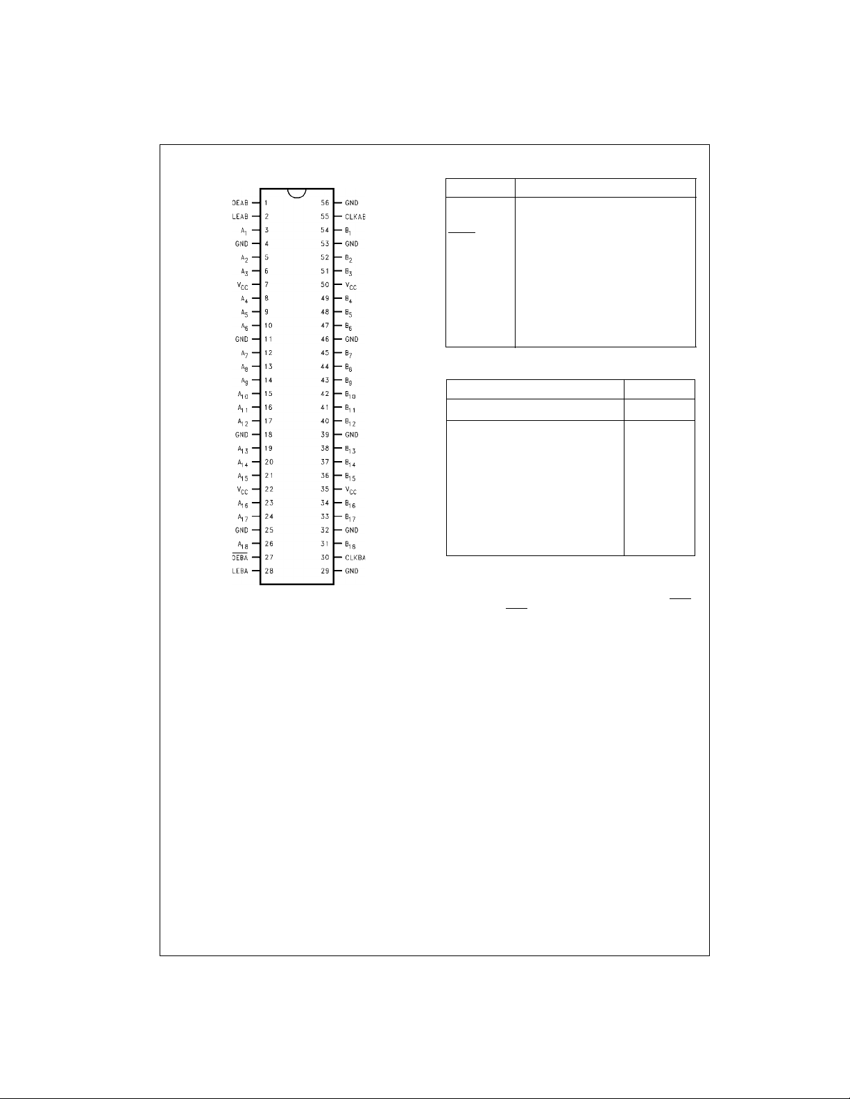
Connection Diagram Pin Descriptions
Pin Names Descriptio n
OEAB Output Enable Input for A to B Direction
74ALVC16501
OEBA
LEAB, LEBA Latch Enable Inputs
CLKAB,
CLKBA
A
1–A18
B
1–B18
(Active HIGH)
Output Enable Input for B to A Direction
(Active LOW )
Clock Inputs
Side A Inputs or 3-STATE Outputs
Side B Inputs or 3-STATE Outputs
Function Table
(Note 2)
Inputs Outputs
OEAB LEAB CLKAB
A
n
B
n
LXXX Z
HHXL L
HHXH H
HL
↑ LL
HL↑ HH
HLHXB
HLLXB
H = HIGH Voltage Level
L = LOW Voltage Level
X = Immaterial (HIGH or LOW, inputs may not float)
Z = High Impedance
Note 2: A-to-B data flow is shown; B-to-A flow is similar but uses OEBA
LEBA and CLKBA. OEBA
Note 3: Output level be fore the indicated steady-s tate input conditions
were established.
Note 4: Output level be fore the indicated steady-s tate input conditions
were established, prov ided that CLK AB was HIGH before LEAB went LOW.
is active LOW.
(Note 3)
0
(Note 4)
0
,
www.fairchildsemi.com 2
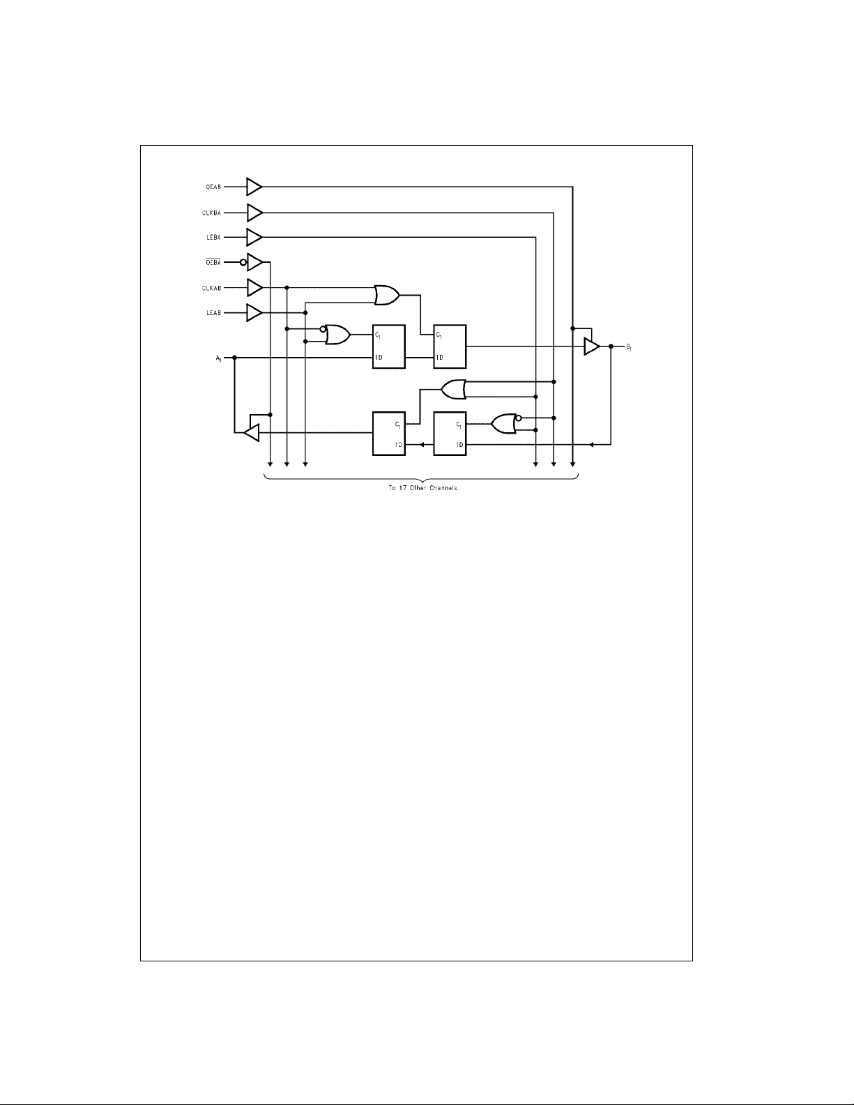
Logic Diagram
74ALVC16501
3 www.fairchildsemi.com
 Loading...