

Fairchild Semiconductor 74ALVC16374 Datasheet
74ALVC16374
Low Voltage 16-Bit D-Type Flip-Flop
with 3.6V Tolerant Inputs and Outputs
74ALVC16374 Low Voltage 16-Bit D-Type Flip-Flop with 3.6V Tolerant Inputs and Outputs
October 2001
Revised October 2001
General Description
The ALVC16374 contains sixteen no n-in ver ti ng D-ty pe f l ipflops with 3-STATE outputs and is intended for bus oriented
applications. The device is byte controlled. A buffered clock
(CP) and output enable (OE
can be shorted together for full 16-bit operation.
The 74ALVC16374 is designed for low voltage (1.65V to
3.6V) V
The 74ALVC16374 is fabricated w ith an advanc ed CMOS
technology to achieve high speed operation while maintaining low CMOS power dissipation.
applications with I/O compatibility up to 3.6V.
CC
) are common t o ea ch b yte an d
Features
■ 1.65V - 3.6V VCC supply operation
■ 3.6V tolerant inputs and outputs
■ t
PD
3.5 ns max for 3.0V to 3.6V V
4.4 ns max for 2.3V to 2.7V V
7.8 ns max for 1.65V to 1.95V V
■ Power-off high impedance inputs and outputs
■ Supports live insertion and withdrawal (Note 1)
■ Uses patented noise/EMI reductio n circuitr y
■ Latchup conforms to JEDEC JED78
■ ESD performance:
Human body model
Machine model
■ Also packaged in plastic Fine-Pitch Ball Grid Array
(FBGA)
Note 1: To ensure the high-impedance state d uring power up or power
down, OE
should be tied to VCC through a pull-up r esistor; the min imum
value of the res istor is d eter mine d by the cu rre nt-sou rcin g ca pa bility of t he
driver.
> 200V
Ordering Code:
Order Number Package Number Package Descriptions
74ALVC16374GX
(Note 2)
74ALVC16374MTD
(Note 3)
Note 2: BGA package available in Tape and Reel only.
Note 3: Devices also available in Tape and Reel. Specify by appending suffix letter “X” to the ordering code.
BGA54A 54-Ball Fine-Pitch Ball Grid Array (FBGA), JEDEC MO-205, 5.5mm Wide
[TAPE and REEL]
MTD48 48-Lead Thin Shrink Small Outline Package (TSSOP), JEDEC MO-153, 6.1mm Wide
CC
CC
CC
> 2000V
© 2001 Fairchild Semiconductor Corporation DS500692 www.fairchildsemi.com
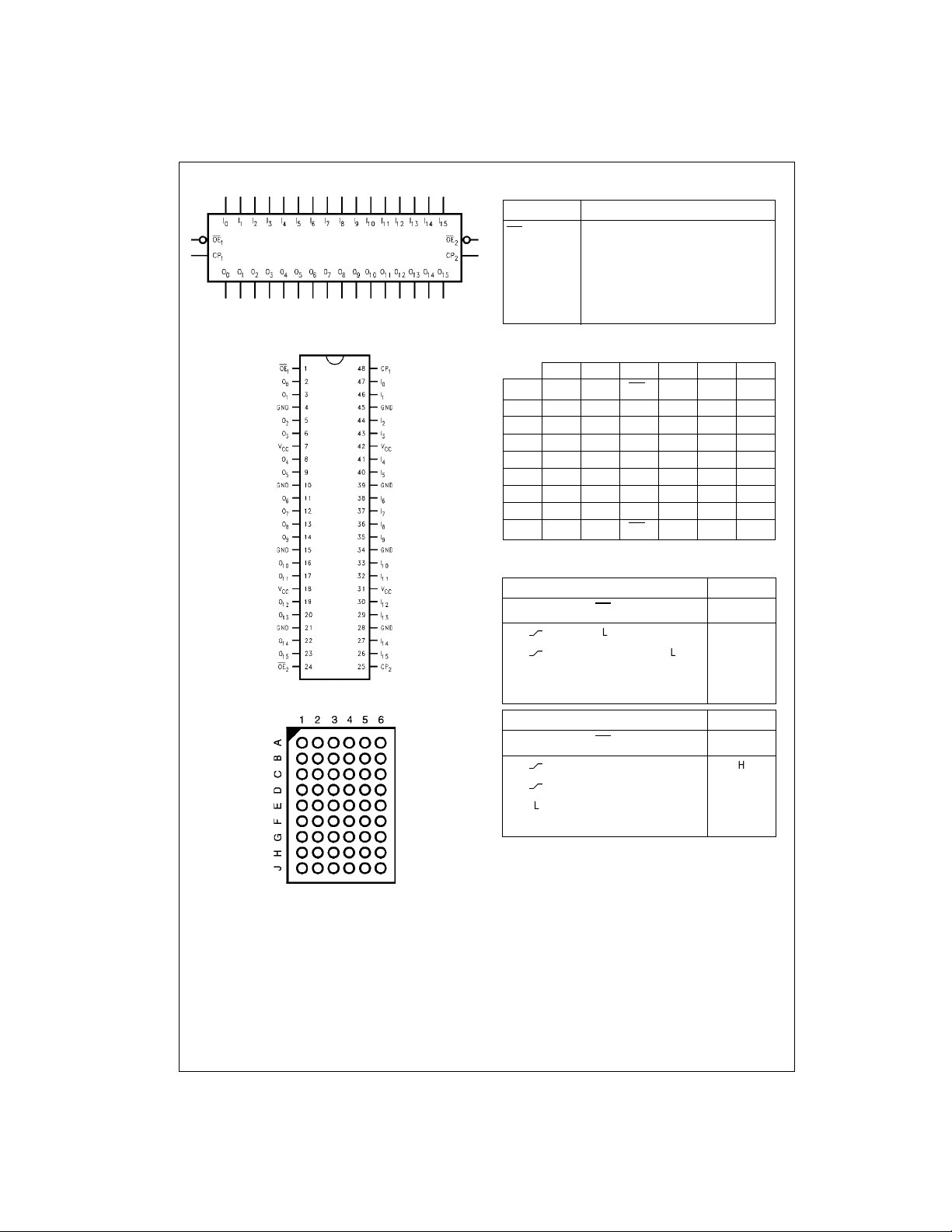
Logic Symbol
74ALVC16374
Connection Diagrams
Pin Assignment for TSSOP
Pin Assignment for FBGA
(Top Thru View)
Pin Descriptions
Pin Names Description
OE
CP
I
0–I15
O
0–O15
n
n
Output Enable Input (Active LOW)
Clock Pulse Input
Inputs
Outputs
NC No Connect
FBGA Pin Assignments
123456
A O
NC OE1CP1NC I
0
B O2O1NC NC I
C O4O3V
CCVCCI3
D O6O5GND GND I
E O8O7GND GND I
F O
G O12O11V
H O14O
J O
O9GND GND I
10
CCVCCI11I12
NC NC I
13
NC OE2CP2NC I
15
13I14
Truth Tables
Inputs Outputs
CP
1
LLXO
XHXZ
CP
2
LLXO
XHXZ
H = HIGH Voltage Level
L = LOW Voltage Level
X = Immaterial (HIGH or LOW, inputs may not float)
Z = High Impedance
= Previous O0 before HIGH-to-LOW of CP
O
0
OE
1
I0–I
7
LHH
LLL
Inputs Outputs
OE
2
I8–I
15
LHH
LLL
1
5
7
9I10
O0–O
0
O8–O
0
0
I
2
I
4
I
6
I
8
15
7
15
www.fairchildsemi.com 2
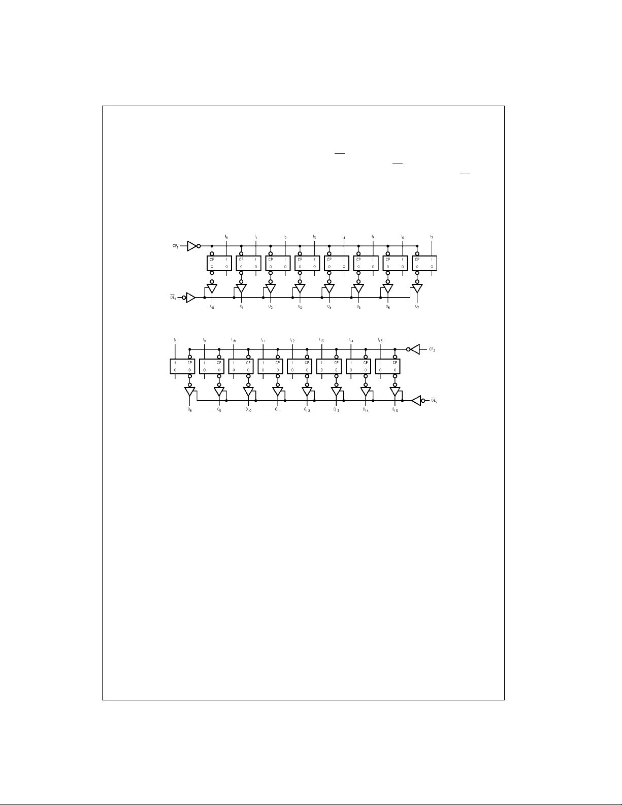
Functional Description
The 74ALVC16374 consists of sixteen edge-triggered
flip-flops with individual D-type inputs and 3-STATE true
outputs. The device i s byte contr olled wit h each byte func tioning identically, but independent of the other. The control
pins can be shorted to gether to obtain f ull 1 6-b it o per ati o n.
Each clock has a buffered clock and buffered Output
Enable common to all flip-flops within that byte. The
description which follows applies to each byte. Each
Logic Diagram
Byte 1 (0:7)
Byte 2 (8:15)
flip-flop will store the state of their individual I inputs that
meet the setup and hold time requirements on the
LOW-to-HIGH Clock (CP
Enable (OE
able at the outputs. Wh en OE
the high impedance state. Operations of the OE
does not affect the state of the flip-flops.
) LOW, the contents of the flip-flops are avail-
n
) transition. With the Output
n
is HIGH, the outputs go to
n
input
n
74ALVC16374
Please note that this diagram is provided only for the understanding of logic operations and should not be used to estimate propagation delays.
3 www.fairchildsemi.com
 Loading...