Fairchild Semiconductor 74ALVC163245 Datasheet

November 2001
Revised November 2001
74ALVC163245
Low Voltage 16-Bit Dual Supply Translating Transceiver
with 3-STATE Outputs
74ALVC163245 Low Voltage 16-Bit Dual Supply Translating Transceiver with 3-STATE Outputs
General Description
The ALVC163245 is a dual supply, 16-bit translating transceiver that is designed for 2 way asynchr onous communication between busses at different supply voltages by
providing true sign al tr ans lati on . T he sup ply r ai ls co nsi st of
V
, which is a higher pote ntial rail operatin g at 2.3V to
CCA
3.6V and V
1.65V to 2.7V. (V
for proper device operation). This dual supply design
allows for t r an s lat i on f ro m 1. 8 V t o 2. 5V b uss e s to bu s ses a t
a higher potential, up to 3.3V.
The Transmit/Receive (T/R
of data flow. Transmit (active-HIGH) enables data from
A Ports to B Ports; Receive (active-LOW) enables data
from B Ports to A Ports. The Output Enable (OE
when HIGH, disable s both A and B Ports by pla cing them
in a High-Z condition. T he A Port interfaces with the h igh er
voltage bus (2.7V to 3.3 V); The B Port inter faces with the
lower voltage bus (1.8V to 2. 5V). Al so the ALVC163245 is
designed so that the control pins (T/R
by V
CCB
The 74ALVC163245 is suitable for mix ed voltage applications such as notebook compute rs using a 1.8V CPU and
3.3V peripheral components. It is fabricated with an
Advanced CMOS technology to achieve high speed operation while maintaining low CMOS power dissipation.
, which is the lower potential rail operating at
CCB
.
must be less than or equal to V
CCB
) input determines the direct ion
, OEn) are supplied
n
) input,
Features
■ Bidirectional interface between busses ranging from
1.65V to 3.6V
■ Supports Live Insertion and Withdrawal (Note 1)
■ Uses patented Quiet Series
circuitry
■ Functionally compatible with 74 series 16245
CCA
■ Latchup conforms to JEDEC JED78
■ ESD performance:
Human Body Model
Machine model
■ Also packaged in plastic Fine-Pitch Ball Grid Array
(FBGA) (Preliminary)
Note 1: To ensure the high impedance state during power up or power
should be tied to V
down, OE
n
value of the resistor is dete rmined by the curren t sourcing capabilit y of the
driver.
>200V
Ordering Code:
Order Number Package Number Package Description
74ALVC163245GX
(Note 2)
74ALVC163245T
(Note 3)
Note 2: BGA package available in Tape and Reel only.
Note 3: Device also available in Tape and Reel. Spe cify by appending the s uffix let t er “X” to the ordering code.
BGA54A
(Preliminary)
MTD48 48-Lead Thi n Shrink Small Outline Package (TSSOP ), JEDEC MO-153, 6.1mm Wide
54-Ball Fine-Pitch Ball Grid Array (FBGA), JEDEC MO-205, 5.5mm Wide
[Tape and Reel]
noise/EMI reduction
>2000V
through a pull up resistor. The minimum
CCB
Quiet Series is a tra demark of Fairchild Semiconductor Corp oration.
© 2001 Fairchild Semiconductor Corporation ds500695 www.fairchildsemi.com

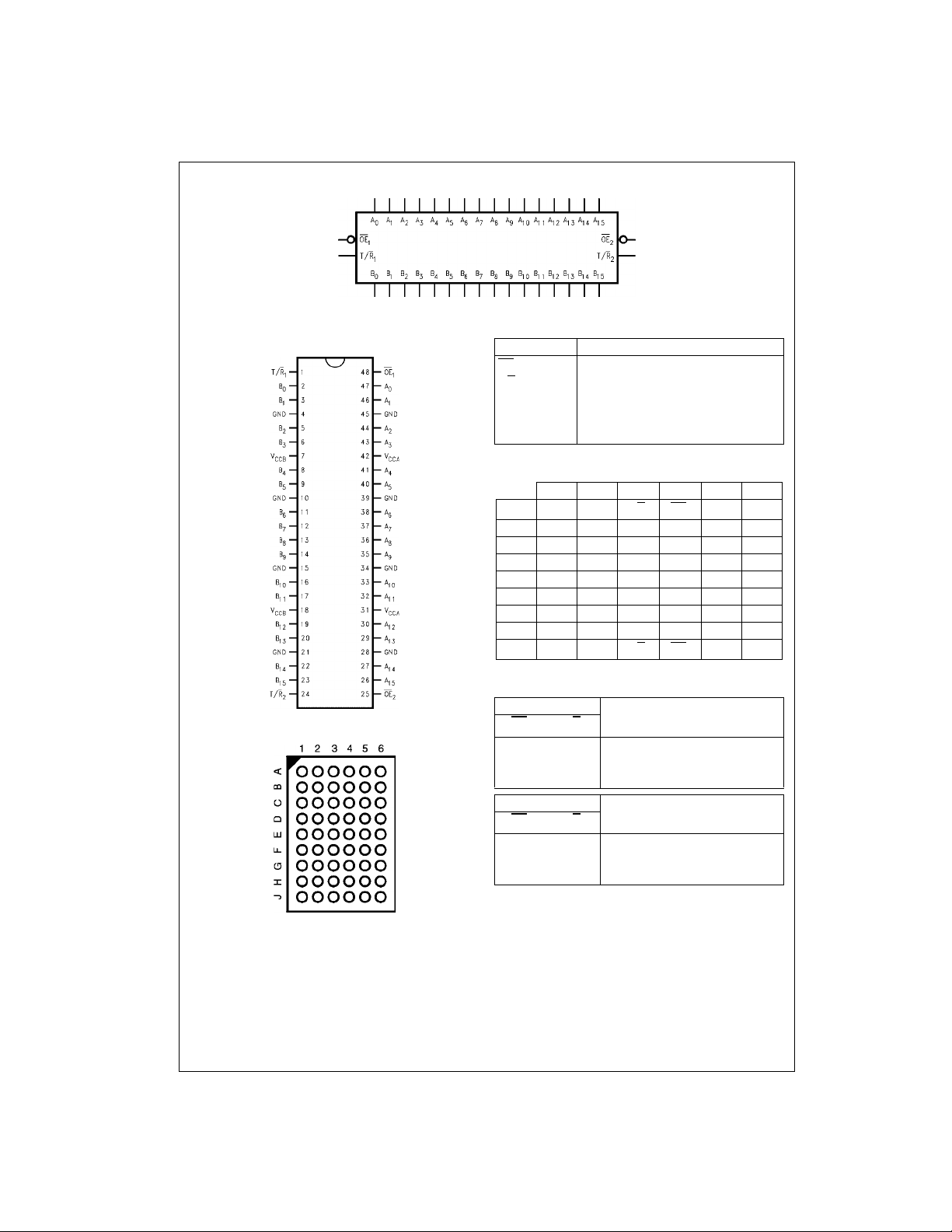
Logic Diagram
74ALVC163245
Connection Diagrams
Pin Assignment for TSSOP
Pin Assignment for FBGA
(Top Thru View)
Pin Descriptions
Pin Names Description
OE
T/R
A
0–A15
B
0–B15
n
n
Output Enable Input (Active LOW)
Transmit/Receive Input
Side A Inputs or 3-STATE Outputs
Side B Inputs or 3-STATE Outputs
NC No Connect
FBGA Pin Assignments
123 456
A B
B B
C B
D B
E B
F B
G B
H B
J B
NC T/R1OE1NC A
0
B
2
4
6
8
10
12B11VCCBVCCAA11
14B13
15
NC NC A
1
B3V
CCBVCCAA3
B5GND GND A
B7GND GND A
B9GND GND A
NC NC A
NC T/R2OE2NC A
Truth Tables
Inputs
OE
T/R
1
1
L L Bus B0–B7 Data to Bus A0–A
L H Bus A0–A7 Data to Bus B0–B
H X HIGH Z State on A0–A7, B0–B
Inputs
OE
T/R
2
2
L L Bus B8–B15 Data to Bus A8–A
L H Bus A8–A15 Data to Bus B8–B
H X HIGH-Z State on A8–A15, B8–B
H = HIGH Voltage Level
L = LOW Voltage Level
X = Immaterial (HIGH or LOW, inputs may not float)
Z = High Impedance
Outputs
Outputs
A
1
A
A
5
A
7
A
9
A
13A14
7
7
7
15
15
15
0
2
4
6
8
10
12
15
www.fairchildsemi.com 2

74ALVC163245 Translator Power Up Sequence Recommendations
To guard against power up problems, some sim ple guidelines need to be adhered to. The 74ALVC163245 is
designed so that the control pins (T/R
by V
. Therefore the first recommendation is to begin by
CCB
powering up the control side of the devic e, V
control pins should b e ramped with or a head of V
, OEn) are supplied
n
. The OE
CCB
CCB
will guard against bus contentions and oscillations as all
A Port and B Port outpu ts will be disabled. To ensure the
high impedance state during power up or power down, OE
should be tied to V
mum value of the resistor is determined by the current
sourcing capability of the driver. Second, the T/R
through a pull up resistor. The mini-
CCB
control
n
pins should be placed at logic LOW (0V) level, this will
ensure that the B-sid e bus pins are config ur ed as i n pu ts to
help guard against bus conten tion and oscillation s. B-side
Data Inputs should be driven to a vali d logic level (0V or
V
), this will prevent excessive current draw and oscilla-
CCB
, this
n
tions. V
V
CCA
can then be power ed up after V
CCA
must be greater than or equal to V
proper device operation. U pon completion of these steps
the device can then be config ured for the users desired
n
operation. Following these steps will help to prevent possible damage to the translator device as well as other system
components.
CCB
CCB
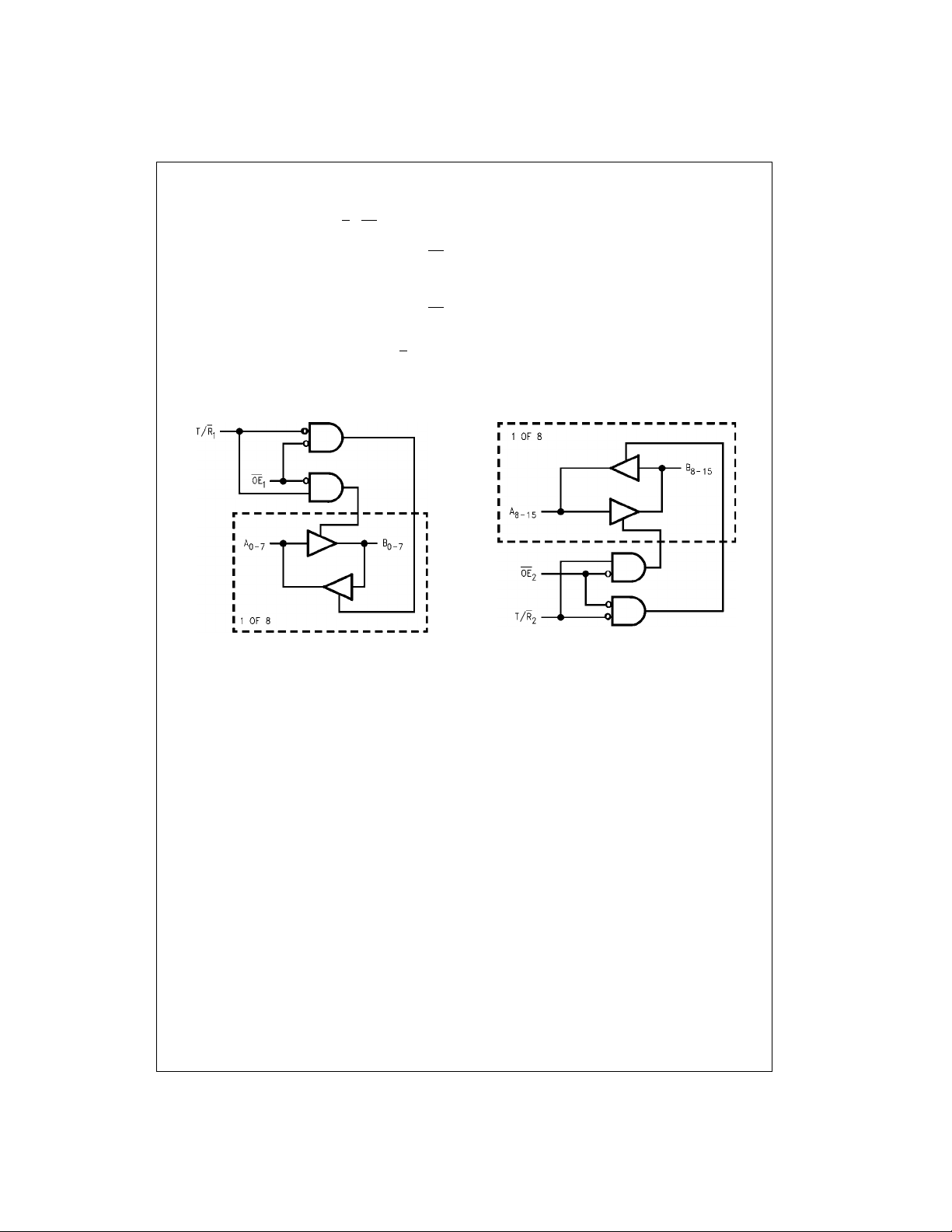
Logic Diagrams
74ALVC163245
, however
to ensure
Please note that thes e diagrams are provided only for the underst anding of logic opera t ions and should not be used to estimate propagation delays.
3 www.fairchildsemi.com
 Loading...