

Fairchild Semiconductor 74ALVC162838 Datasheet
November 2001
Revised November 2001
74ALVC162838
Low Voltage 16-Bit Selectable Register /Buffer
with 3.6V Tolerant Inputs/Outputs
and 26
Ω Series Resistors in the Outputs
Resistors in the Outputs
74ALVC162838 Low Voltage 16-Bit Selectable Register/Buffer with 3.6V Tolerant Inputs/Outputs and 26
General Description
The ALVC162838 contains sixteen non-inverting selectable
buffered or registered pa ths. T he dev ic e can be c onfi g ur ed
to operate in a regis tered, or flow throu gh buffer mode by
utilizing the register enable (REGE) and Clock (CLK) signals. The device operates in a 16-bit word wide mode. All
outputs can be plac ed into 3-State through the use of the
OE
pin. These devices are ideally suited for buffered or
registered 168 pin and 200 pin SDRAM DIMM memory
modules.
The 74ALVC162838 is designed for l ow voltage (1.6 5V to
3.6V) V
The ALVC162838 is also designed with 26
tors in the outputs. This design reduces line noise in applications such as memory address drivers, clock drivers, and
bus transceivers/transmitters.
The 74ALVC162838 is fabricated with an adva nce d CMOS
technology to achieve high speed operation while maintaining low CMOS power dissipation.
applications with I/O compatibility up to 3.6V.
CC
Ω series resis-
Features
■ Compatible with PC100 and PC133 DIMM module
specifications
■ 1.65V–3.6V V
■ 3.6V tolerant inputs and outputs
■ 26
Ω series resistors in the outputs
■ t
(CLK to On)
PD
4.4 ns max for 3.0V to 3.6V V
5.9 ns max for 2.3V to 2.7V VCC
9.8 ns max for 1.65V to 1.95V V
■ Power-off high impedance inputs and outputs
■ Supports live insertion and withdrawal (Note 1)
■ Uses patented noise/EMI reductio n circuitr y
■ Latchup conforms to JEDEC JED78
■ ESD performance:
Human body model
Machine model
Note 1: To ensure the high-impedance state d uring power up or power
should be tied to VCC through a pull-up resistor. The minimum
down, OE
value of the resistor is determined by the current -sourcing capability of the
driver.
supply operation
CC
> 2000V
> 200V
CC
CC
Ordering Code:
Ordering Code Package Number Package Descriptions
74ALVC162838T MTD48 48-Lead Thin Shrink Small Outline Package (TSSOP), JEDEC MO-153, 6.1mm Wide
Devices also available in Tape and Reel. Specify by appending suffix letter “X” to the ordering code.
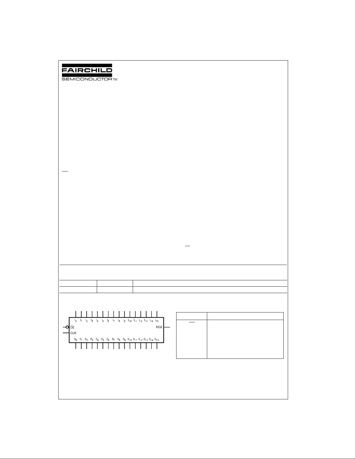
Logic Symbol Pin Descriptions
Pin Names Description
OE
I
0–I15
O
0–O15
CLK Clock Input
REGE Register Enable Input
© 2001 Fairchild Semiconductor Corporation DS500711 www.fairchildsemi.com
Output Enable Input (Active LOW)
Inputs
Outputs
Ω
Series
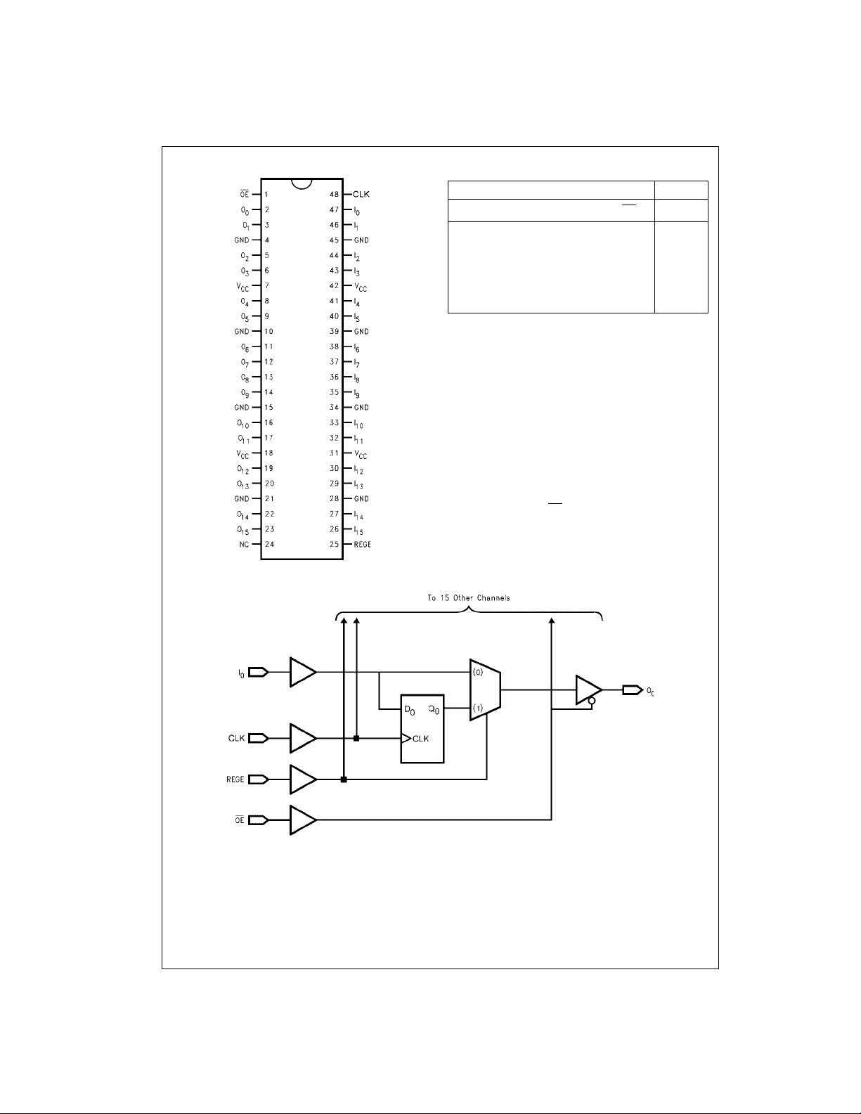
Connection Diagram Truth Table
CLK REGE
↑ HHL H
74ALVC162838
↑ HLL L
XLHLH
XLLLL
XXXHZ
H = Logic HIGH
L = Logic LOW
X = Don’t Care, but not floating
Z = High Impedance
↑ = LOW-to-HIGH Clock Transition
Functional Description
The 74ALVC162838 consists of sixteen selectable noninverting buffers or regist ers with word wi de modes. Mode
functionality is selected through operation of the CLK and
REGE pin as shown by the truth table. When REGE is held
at a logic HIGH the device oper ates as a 16-bit register.
Data is transferred from I
CLK input. When the REG E pin i s held a t a l ogic LOW the
device operates in a flow through mode and data propagates directly from the I to the O outputs. All outputs can be
3-stated by holding the OE
Inputs Outputs
I
n
to On on the rising edge of the
n
pin at a logic HIGH.
OE
O
n
Logic Diagram
www.fairchildsemi.com 2
 Loading...