

Fairchild Semiconductor 74ALVC162601 Datasheet
September 2001
Revised October 2001
74ALVC162601
Low Voltage 18-Bit Universal Bus Transceivers
with 3.6V Tolerant Inputs and Outputs
and 26
Ω Series Resistors in the B-Port Outputs
Series Resistors in the B-Port Outputs
74ALVC162601 Low Voltage 18-Bit Universal Bus Transceivers with 3.6V Tolerant Inputs and Outputs and 26
General Description
The 74ALVC162601, 18-bit universal bus transceiver, combines D-type latches and D-type flip-flops to allow data flow
in transparent, latched, and clocked modes.
Data flow in each dir ection is controlled by output-enable
(OEAB
and OEBA), latch-enable (LEAB and LEBA), and
clock (CLKAB and CLKBA) inputs. The clock can be controlled by the clock-enable (CLKENAB
inputs. For A-to-B data flow, the device operates in the
transparent mode when LEAB is HIGH. When LEAB is
LOW, the A data is latched if CLKAB is held at a HIGH-toLOW logic level. If LEA B is LOW, the A bus data is s tored
in the latch/flip-flop on the LOW-to-HIGH transition of
CLKAB. Output-enable OEAB
is HIGH, the outputs are in the HIGH-impedance state.
Data flow for B to A is similar to tha t of A to B but uses
OEBA
, LEBA, CLKBA and CLKENBA.
The 74ALVC162601 is designed for l ow voltage (1.6 5V to
3.6V) V
The 74ALVC162601 is also designed with 26
resistors in the B-Port outp uts. This design reduces line
noise in applications such as memory address drivers,
clock drivers, and bus transceivers/transmitters.
applications with I/O compatibility up to 3.6V.
CC
is active-LOW. When OEAB
and CLKENBA)
Ω series
Features
■ 1.65V–3.6V VCC supply operation
■ 3.6V tolerant inputs and outputs
■ 26
Ω series resistors in B-Port outputs
■ t
(A to B)
PD
4.3 ns max for 3.0V to 3.6V V
5.1 ns max for 2.3V to 2.7V V
9.2 ns max for 1.65V to 1.95V V
■ Power-down high impedance inputs and outputs
■ Supports live insertion/withdrawal (Note 1)
■ Uses patented noise/EMI reductio n circuitr y
■ Latchup conforms to JEDEC JED78
■ ESD performance:
Human body model
Machine model
Note 1: To ensure the high-impedance state d uring power up or power
should be tied to VCC through a pull-up r esistor; the min imum
down, OE
value of the res istor is d eter mine d by the cu rre nt-sou rcin g ca pa bility of t he
driver.
>200V
CC
CC
CC
> 2000V
Ordering Code:
Order Number
74ALVC162601T MTD56 56-Lead Thin Shrink Small Outline Package (TSSOP), JEDEC MO-153, 6.1mm Wide
Devices also availab l e in Tape and Reel. Specify by appending th e s uffix let t er “X” to the ordering code.
Package
Number
Package Description
© 2001 Fairchild Semiconductor Corporation DS500676 www.fairchildsemi.com
Ω

Pin Descriptions
Pin Names Description
OEAB
, OEBA Output Enable Inputs
LEAB, LEBA Latch Enable Inputs
74ALVC162601
CLKAB, CLKBA Clock Inputs
CLKENAB
A
B
, CLKENBA Clock Enable Inputs
1–A18
1–B18
(Active LOW)
Side A Inputs
or 3-STATE Outputs
Side B Inputs
or 3-STATE Outputs
Connection Diagram
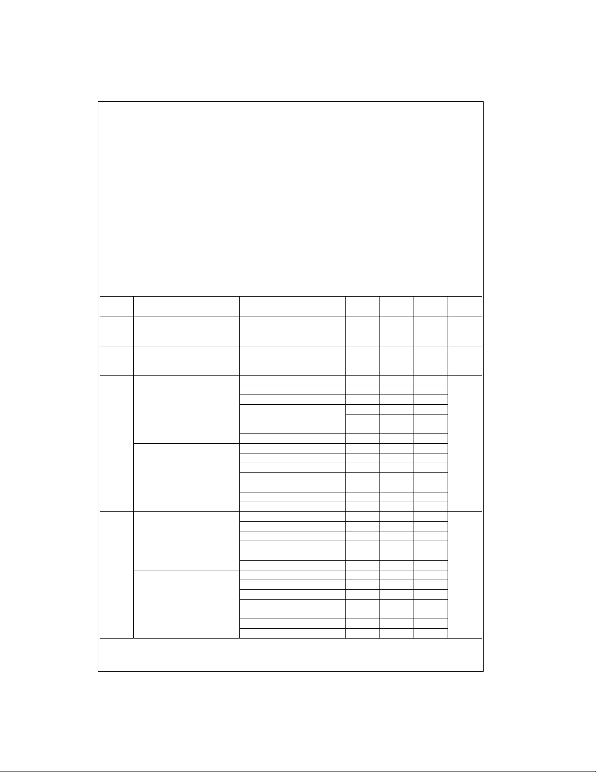
Function Table
(Note 2)
Inputs Outputs
CLKENAB
OEAB LEAB CLKAB A
B
n
n
XHXXXZ
XLHXLL
XLHXHH
HLLXXB
HLLXXB
LLL
LLL
↑ LL
↑ HH
LLLLXB
LLLHXB
H = HIGH Voltage Level
L = LOW Voltage Level
X = Immaterial (HIGH or LOW, inputs may not float)
Z = High Impedance
Note 2: A-to-B data flow is shown; B-to-A flow is s imilar but use s OEBA
LEBA, CLKBA, and CLKENBA
Note 3: Output level before the indicated steady-state input conditions
were established.
Note 4: Output level befor e the indicated steady-state input conditions
were established, provided that CLKAB was HIGH before LEAB went LOW.
.
(Note 3)
0
(Note 3)
0
(Note 3)
0
(Note 4)
0
Logic Diagram
,
www.fairchildsemi.com 2
Absolute Maximum Ratings(Note 5) Recommended Operating
Supply Voltage (VCC) −0.5V to +4.6V
DC Input Voltage (V
Output Voltage (V
DC Input Diode Current (I
V
< 0V −50 mA
I
DC Output Diode Current (I
< 0V −50 mA
V
O
) −0.5V to 4.6V
I
) (Note 6) −0.5V to VCC +0.5V
O
)
IK
)
OK
DC Output Source/Sink Current
(I
) ±50 mA
OH/IOL
or GND Current per
DC V
CC
Supply Pin (I
Storage Temperature Range (T
or GND) ±100 mA
CC
) −65°C to +150°C
STG
Conditions
Power Supply
Operating 1.65V to 3.6V
Input Voltage 0V to V
Output Voltage (VO)0V to V
Free Air Operating Temperature (TA) −40°C to +85°C
Minimum Input Edge Rate (
= 0.8V to 2.0V, VCC = 3.0V 10 ns/V
V
IN
Note 5: The Absolute Maxi mum Ratings are thos e values beyond which
the safety of the d evice cannot b e guaranteed . The device sh ould not be
operated at these limit s. The parametric values defi ned in the Electrical
Characteristics tables are not guaranteed at the Absolute Maximum Ratings. The “Recommended Operating Conditions” table will define the conditions for actual device oper ation.
Absolute Maximum Rating must be observed.
Note 6: I
O
Note 7: Floating or unused control inputs must be held HIGH or LOW.
(Note 7)
∆t/∆V)
DC Electrical Characteristics
V
Symbol Parameter Conditions
V
IH
V
IL
V
OH
V
OL
HIGH Level Input Voltage 1.65 - 1.95 0.65 x V
LOW Level Input Voltage 1.65 - 1.95 0.35 x V
HIGH Level Output Voltage IOH = −100 µA 1.65 - 3.6 VCC - 0.2
A Outputs IOH = −4 mA 1.65 1.2
HIGH Level Output Voltage IOH = −100 µA 1.65 - 3.6 VCC - 0.2
B Outputs I
LOW Level Output Voltage IOL = 100 µA 1.65 - 3.6 0.2
A Outputs IOL = 4 mA 1.65 0.45
LOW Level Output Voltage IOL = 100 µA 1.65 - 3.6 0.2
B Outputs IOL = 2 mA 1.65 0.45
I
= −6 mA 2.3 2.0
OH
= −12 mA 2.3 1.7
I
OH
IOH = −24 mA 3.0 2
= −2 mA 1.65 1.2
OH
= −4 mA 2.3 1.9
I
OH
IOH = −6 mA 2.3 1.7
IOH = −8 mA 2.7 2
IOH = −12 mA 3.0 2
IOL = 6 mA 2.3 0.4
IOL = 12 mA 2.3 0.7
IOL = 24 mA 3.0 0.55
IOL = 4 mA 2.3 0.4
IOL = 6 mA 2.3 0.55
IOL = 8 mA 2.7 0.6
IOL = 12 mA 3.0 0.8
CC
(V)
2.7 - 3.6 2.0
2.7 - 3.6 0.8
2.7 2.2
3.0 2.4
3.0 2.4
2.7 0.4
3.0 0.55
Min Max Units
CC
74ALVC162601
CC
CC
V2.3 - 2.7 1.7
CC
V2.3 - 2.7 0.7
V
V
3 www.fairchildsemi.com
 Loading...