

Fairchild Semiconductor 74ALVC16240 Datasheet
October 2001
Revised October 2001
74ALVC16240
Low Voltage 16-Bit Inverting Buffer/Line Driver
with 3.6V Tolerant Inputs and Outputs
74ALVC16240 Low Voltage 16-Bit Inverting Buffer/Line Driver with 3.6V Tolerant Inputs and Outputs
General Description
The ALVC16240 contains sixteen inverting buffers w ith 3STATE outputs to be employe d as a mem ory and a ddress
driver, clock driver, or bus oriented transmitter/receiver.
The device is nibble (4-bit) controlled. Each nibble has separate 3-STATE control inputs which can be shorted
together for full 16-bit operation.
The 74ALVC16240 is designed for low voltage (1.65V to
3.6V) V
The 74ALVC16240 is fabricated w ith an advanc ed CMOS
technology to achieve high speed operation while maintaining low CMOS power dissipation.
applications with I/O capability up to 3.6V.
CC
Features
■ 1.65V to 3.6V VCC supply operation
■ 3.6V tolerant inputs and outputs
■ t
PD
3.0 ns max for 3.0V to 3.6V V
3.5 ns max for 2.3V to 2.7V VCC
6.0 ns max for 1.65V to 1.95V V
■ Power-off high impedance inputs and outputs
■ Supports live insertion and withdrawal (Note 1)
■ Uses patented noise/EMI reductio n circuitr y
■ Latchup conforms to JEDEC JED78
■ ESD performance:
Human body model
Machine model
Note 1: To ensure the high-impedance state d uring power up or power
down, OE
should be tied to VCC through a pull-up r esistor; the min imum
value of the res istor is d eter mine d by the cu rre nt-sou rcin g ca pa bility of t he
driver.
> 200V
CC
CC
> 2000V
Ordering Code:
Order Number Package Number Package Descriptions
74ALVC16240MTD MTD48 48-Lead Thin Shrink Small Outline Package (TSSOP), JEDEC MO-153, 6.1mm Wide
Devices also availab le in Tape and Reel. Specify by appending the suffix letter “X” to the o rdering code.
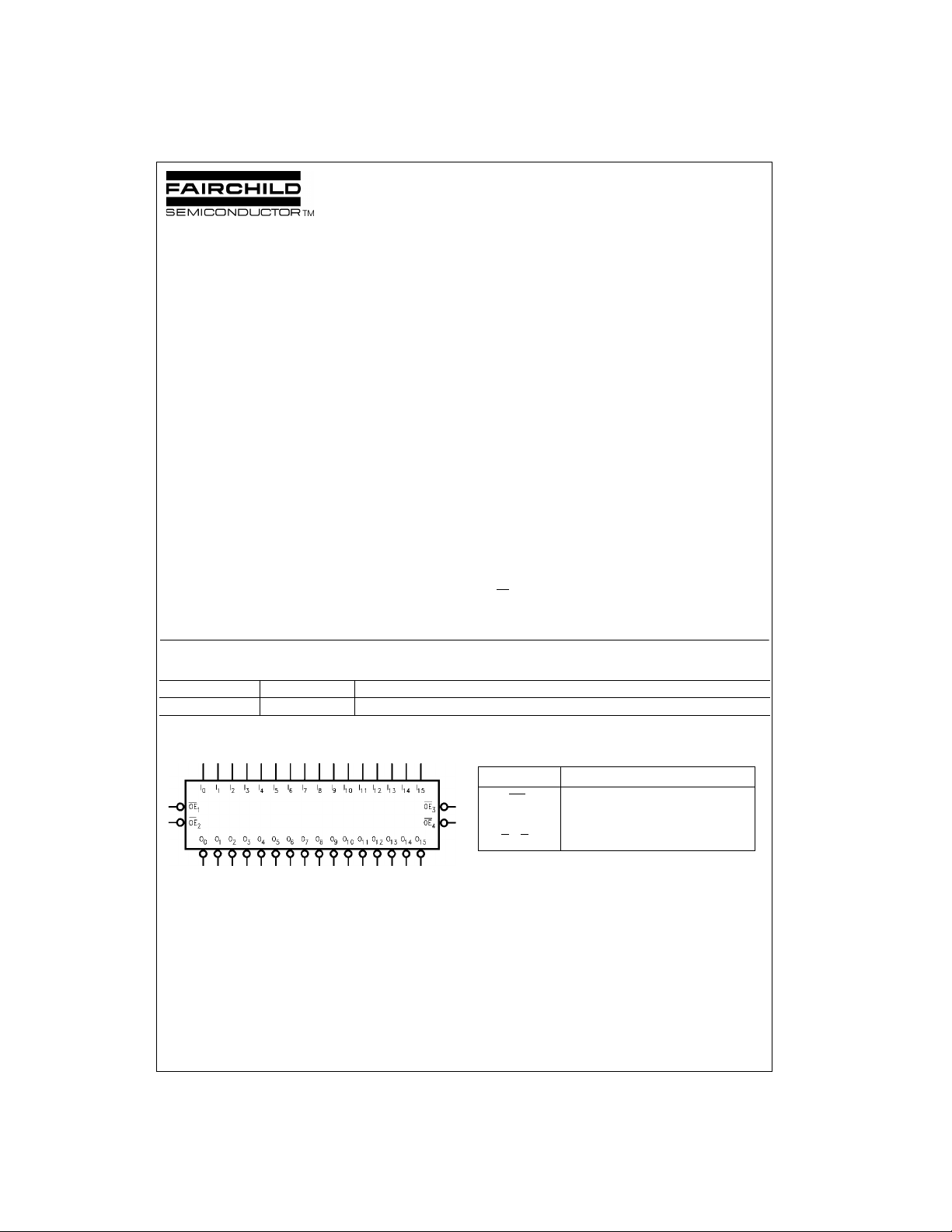
Logic Symbol Pin Descriptions
Pin Names Description
OE
I
0–I15
O
0–O15
n
Output Enable Input (Active LOW)
Inputs
Outputs
© 2001 Fairchild Semiconductor Corporation DS500689 www.fairchildsemi.com
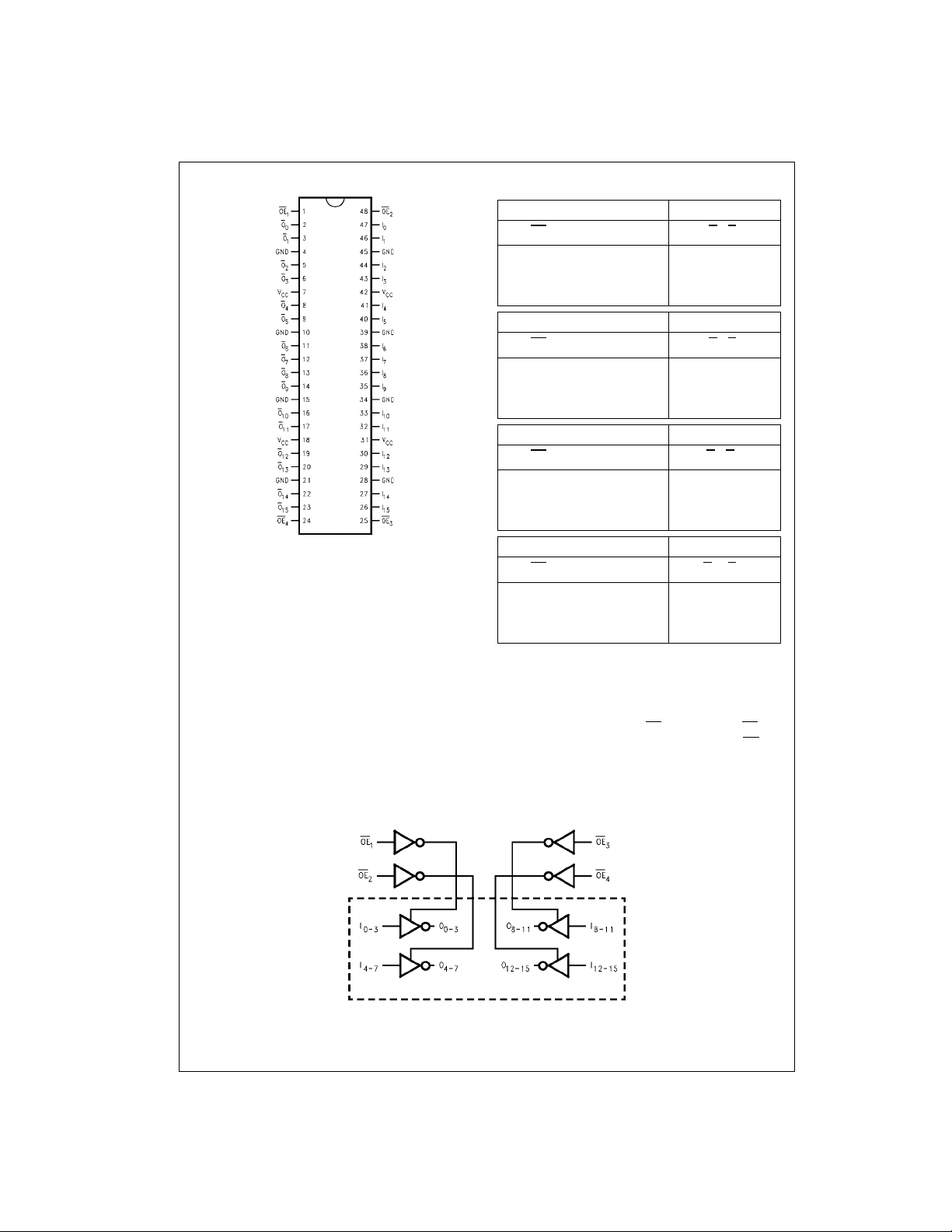
Connection Diagram Truth Tables
OE
74ALVC16240
LL H
LH L
HX Z
OE
LL H
LH L
HX Z
OE
LL H
LH L
HX Z
OE
LL H
LH L
HX Z
H = HIGH Voltage Level
L = LOW Voltage Level
X = Immaterial (HIGH or LOW, inputs may not float)
Z = High Impedance
Inputs Outputs
1
I0–I
3
Inputs Outputs
2
I4–I
7
Inputs Outputs
3
I8–I
11
Inputs Outputs
4
I12–I
15
O0–O
O4–O
O8–O
O12–O
3
7
11
15
Functional Description
The 74ALVC16240 contains sixteen inverting buffers with
3-STATE outputs. The device is nibble (4 bits) controlled
with each nibble funct ioning ide ntically, but independent of
each other. The control pins may be shor ted together to
obtain full 16-bit ope ration.The 3-STATE outputs are con-
Logic Diagram
www.fairchildsemi.com 2
trolled by an Output Enable (OE
LOW, the outputs are in the 2-state mode. When OE
) input. When OEn is
n
is
n
HIGH, the standard outputs are in the high impedance
mode but this does not interfere with entering new data into
the inputs.
 Loading...