

Fairchild Semiconductor 74ALVC162374 Datasheet
74ALVC162374
Low Voltage 16-Bit D-Type Flip-Flop
with 3.6V Tolerant Inputs and Outputs
74ALVC162374 Low Voltage 16-Bit D-Type Flip-Flop
October 2001
Revised October 2001
and 26
General Description
The ALVC162374 contains sixteen non-inverting D-type
flip-flops with 3-STATE outputs and is intended for bus oriented applications. The dev ice is byte controlled. A buffered clock (CP) and ou tput enable (OE
each byte and can be shorted together for full 16-bit operation.
The ALVC162374 is also designed with 26
tors in the outputs. This design reduces line noise in applications such as memory address drivers, clo ck drive rs and
bus transceivers/transmitters.
The 74ALVC162374 is designed for l ow voltage (1.6 5V to
3.6V) V
The 74ALVC162374 is fabricated with an adva nce d CMOS
technology to achieve high speed operation while maintaining low CMOS power dissipation.
Ω Series Resistors in Outputs
) are common to
Ω series resis-
applications with I/O compatibility up to 3.6V.
CC
Features
■ 1.65V–3.6V VCC supply operation
■ 3.6V tolerant inputs and outputs
■ 26
Ω series resistors in outputs
■ t
(CLK to On)
PD
3.9 ns max for 3.0V to 3.6V V
5.3 ns max for 2.3V to 2.7V V
9.6 ns max for 1.65V to 1.95V V
■ Power-off high impedance inputs and outputs
■ Supports live insertion and withdrawal (Note 1)
■ Uses patented noise/EMI reductio n circuitr y
■ Latchup conforms to JEDEC JED78
■ ESD performance:
Human body model
Machine model
Note 1: To ensure the high-impedance state d uring power up or power
should be tied to VCC through a pull-up r esistor; the min imum
down, OE
value of the res istor is d eter mine d by the cu rre nt-sou rcin g ca pa bility of t he
driver.
> 200V
CC
CC
CC
> 2000V
Ordering Code:
Order Number Package Number Package Descriptions
74ALVC162374T MTD48 48-Lead Thin Shrink Small Outline Package (TSSOP), JEDEC MO-153, 6.1mm Wide
Devices also available in Tape and Reel. Specify by appending suffix letter “X” to the ordering co de.
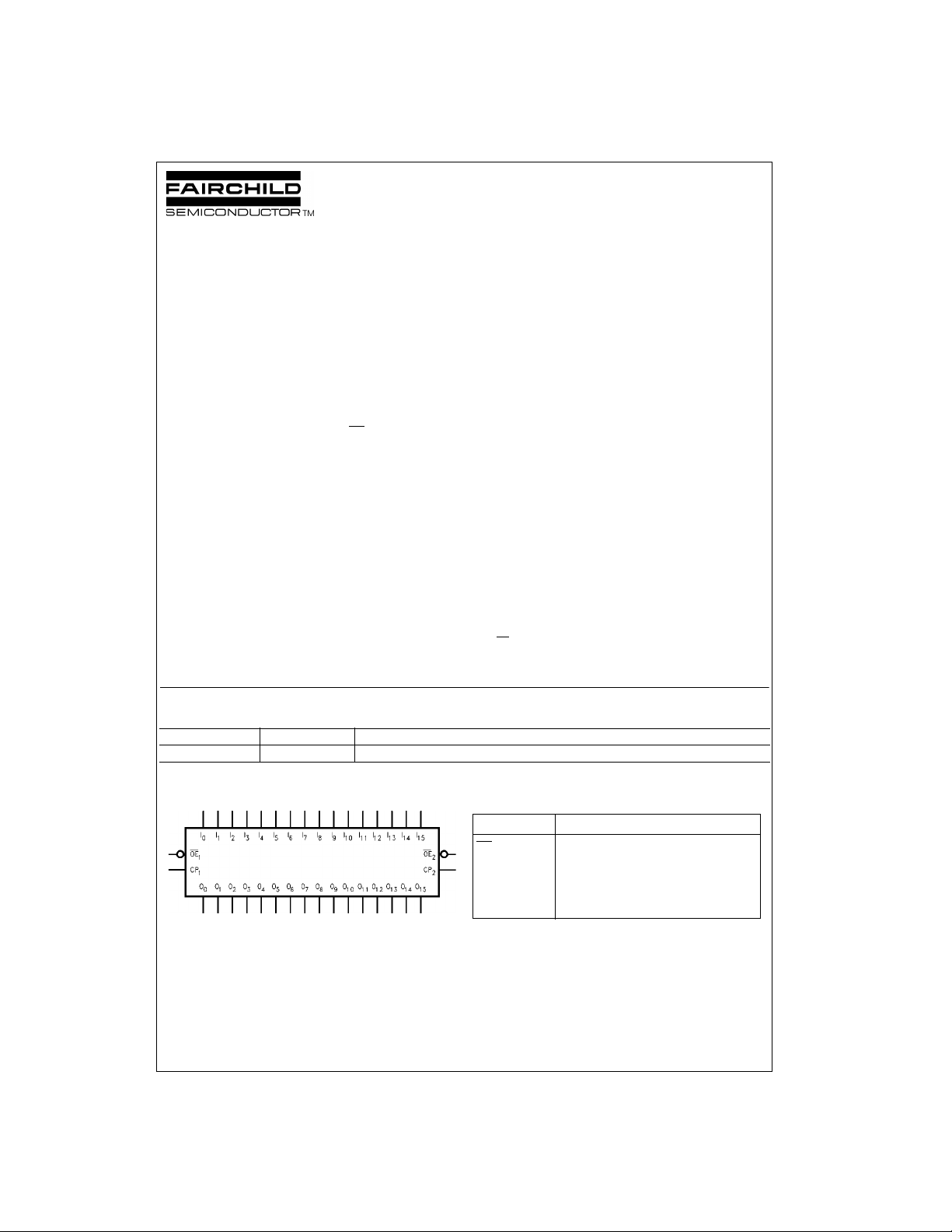
Logic Symbol Pin Descriptions
Pin Names Description
OE
n
CP
n
I
0–I15
O
0–O15
© 2001 Fairchild Semiconductor Corporation DS500688 www.fairchildsemi.com
Output Enable Input (Active LOW)
Clock Pulse Input
Inputs
Outputs

Connection Diagram Truth Tables
CP
74ALVC162374
CP
H = HIGH Voltage Level
L = LOW Voltage Level
X = Immaterial (HIGH or LOW, inputs may not float)
Z = High Impedance
= Previous O0 before HIGH-to-LOW of CP
O
0
Functional Description
The 74ALVC162374 consists of sixteen edge-triggered flipflops with individua l D-type inputs and 3-STATE true outputs. The device is byt e co ntro l led w ith e ach byte fun ctioning identically, but independ ent of the other. The control
pins can be shor ted tog eth er to ob tai n fu ll 16 -b it o per ati o n.
Each clock has a buffered clock and buffered Output
Enable common to all flip-flops within that byte. The
description which follows applies to each b yte. Each flip-
flop will store the state of their ind ividual I inputs that m eet
the setup and hold time requirements on the LOW-to-HIGH
Clock (CP
n
the contents of the flip-flops are available at th e outputs.
When OE
n
state. Operations of the OE
of the flip-flops.
Inputs Outputs
OE
1
LHH
LLL
LLXO
I0–I
1
O0–O
7
7
0
XHXZ
Inputs Outputs
OE
2
LHH
LLL
LLXO
I8–I
2
O8–O
15
15
0
XHXZ
) transition. With the Output Enable (OEn) LOW,
is HIGH, the outputs go to the high impedance
input does not affect the state
n
Logic Diagram
Byte 1 (0:7)
Byte 2 (8:15)
Please note that this diagram is provided only for the understanding of logic operations and should not be used to estimate propagation delays.
www.fairchildsemi.com 2
 Loading...