

Fairchild Semiconductor 74ALVC162245 Datasheet
74ALVC162245
Low Voltage 16-Bit Bidirectional Transceiver
with 3.6V Tolerant Inputs and Outputs
and 26
Ω Series Resistors in A Port Outputs
October 2001
Revised November 2001
Series Resistors in A Port Outputs
74ALVC162245 Low Voltage 16-Bit Bidirectional Transceiver with 3.6V Tolerant Inputs and Outputs and 26
General Description
The ALVC162245 contains sixteen non-inverting bidirectional buffers with 3-STATE outputs and is intended for bus
oriented applications. The device is byte control led. Each
byte has separate 3-STATE control inputs which can be
shorted together for full 16-bit operation. Th e T/R
determine the dire ction of data flow through the device.
The OE
inputs disable both th e A and B Ports by placing
them in a high impedance state.
The 74ALVC162245 is designed for l ow voltage (1.6 5V to
3.6V) V
The 74ALVC162245 is also designed with 26
resistance in the A Port outputs. This design r educes line
noise in applications such as memory address drivers,
clock drivers, and bus transceivers/transmitters.
The 74ALVC162245 is fabricated with an adva nce d CMOS
technology to achieve high speed operation while maintaining low CMOS power dissipation.
applications with I/O compatibility up to 3.6V.
CC
inputs
Ω series
Features
■ 1.65V–3.6V VCC supply operation
■ 3.6V tolerant inputs and outputs
■ 26
Ω series resistors in A Port outputs
■ t
PD
3.9 ns max for 3.0V to 3.6V V
4.8 ns max for 2.3V to 2.7V V
8.6 ns max for 1.65V to 1.95V V
■ Power-down high impedance inputs and outputs
■ Supports live insertion/withdrawal (Note 1)
■ Uses patented noise/EMI reductio n circuitr y
■ Latchup conforms to JEDEC JED78
■ ESD performance:
Human body model
Machine model
Note 1: To ensure the high-impedance state d uring power up or power
down, OE
should be tied to VCC through a pull-up r esistor; the min imum
value of the res istor is d eter mine d by the cu rre nt-sou rcin g ca pa bility of t he
driver.
>200V
CC
CC
CC
> 2000V
Ordering Code:
Order Number Package Number Package Description
74ALVC162245T MTD48 48-Lead Thin Shrink Small Outline Package (TSSOP), JEDEC MO-153, 6.1mm Wide
Devices also availab l e in Tape and Reel. Specify by appending th e s uffix let t er “X” to the ordering code.
© 2001 Fairchild Semiconductor Corporation DS500679 www.fairchildsemi.com
Ω
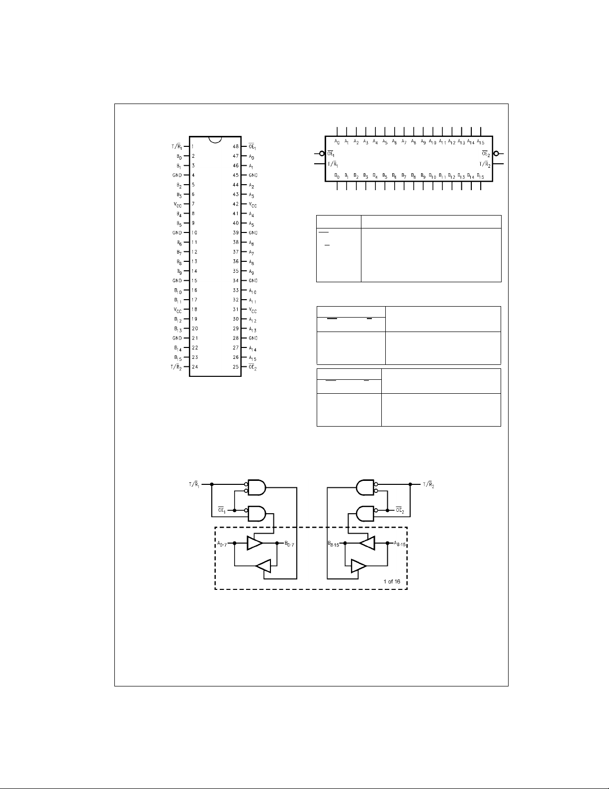
Connection Diagram Logic Symbol
74ALVC162245
Pin Descriptions
Pin Names Description
OE
n
T/R
n
A
0–A15
B
0–B15
Truth Tables
Inputs
OE
1
L L Bus B0–B7 Data to Bus A0–A
L H Bus A0–A7 Data to Bus B0–B
H X HIGH Z State on A0–A7, B0–B
Inputs
OE
2
L L Bus B8–B15 Data to Bus A8–A
L H Bus A8–A15 Data to Bus B8–B
H X HIGH Z State on A8–A15, B8–B
H = HIGH Voltage Level
L = LOW Voltage Level
X = Immaterial (HIGH or LOW, inputs and I/O’s may not float)
Z = High Impedance
Output Enable Input (Active LOW)
Transmit/Receive Input
Side A Inputs or 3-STATE Outputs
Side B Inputs or 3-STATE Outputs
T/R
T/R
1
2
Outputs
Outputs
7
7
7
15
15
15
Logic Diagram
www.fairchildsemi.com 2
 Loading...