

Fairchild Semiconductor 74ALVC162244 Datasheet
74ALVC162244
Low Voltage 16-Bit Buffer/Line Driver
with 3.6V Tolerant Inputs and Outputs
and 26
General Description
The ALVC162244 contains sixteen non-inverting buffers
with 3-STATE outputs to be employ ed as a memory and
address driver, clock driver, or bus oriented transmitter/
receiver. The device is nibble (4-bit) controlled. Each nibble
has separate 3-STATE control inputs which can be shorted
together for full 16-bit operation.
The 74ALVC162244 is designed for l ow voltage (1.65V to
3.6V) V
74ALVC162244 is also designed with 26
in the outputs. This de sign reduces line noise in app lications such as memory address drivers, clock drivers, and
bus transceivers/transmitters.
The 74ALVC162244 is fabricated with an adva nce d CMOS
technology to achieve high speed operation while maintaining low CMOS power dissipation.
Ω Series Resistor in Outputs
applications with I/O capability up to 3.6V. The
CC
Ω series resistors
Features
■ 1.65V to 3.6V VCC supply operation
■ 3.6V tolerant inputs and outputs
Ω series resistors in outputs
■ 26
■ t
PD
3.8 ns max for 3.0V to 3.6V V
4.3 ns max for 2.3V to 2.7V V
7.6 ns max for 1.65V to 1.95V V
■ Power-off high impedance inputs and outputs
■ Supports live insertion and withdrawal
■ Uses patented noise/EMI reductio n circuitr y
■ Latchup conforms to JEDEC JED78
■ ESD performance:
Human body model
Machine model
■ Also packaged in plastic Fine-Pitch Ball Grid Array
(FBGA)
Note 1: To ensure the high-impedance state d uring power up or power
down, OE
should be tied to VCC through a pull-up r esistor; the min imum
value of the res istor is d eter mine d by the cu rre nt-sou rcin g ca pa bility of t he
driver.
> 2000V
> 200V
November 2001
Revised November 2001
CC
CC
CC
74ALVC162244 Low Voltage 16-Bit Buffer/Line Dri ver with 3.6V T olerant Inputs and Outputs and 26
Resistor in Outputs
Ordering Code:
Order Number Package Number Package Description
74ALVC162244GX
(Note 2)
74ALVC162244T
(Note 3)
Note 2: BGA package available in Tape and Reel only.
Note 3: Devices also available in Tape and Reel. Specify by appending suffix letter “X” to the ordering code.
© 2001 Fairchild Semiconductor Corporation DS500696 www.fairchildsemi.com
BGA54A 54-Ball Fine-Pitch Ball Grid Array (FBGA), JEDEC MO-205, 5.5mm Wide
[TAPE and REEL]
MTD48 48-Lead Thin Shrink Small Outline Package (TSSOP), JEDEC MO-153, 6.1mm Wide
Ω
Series
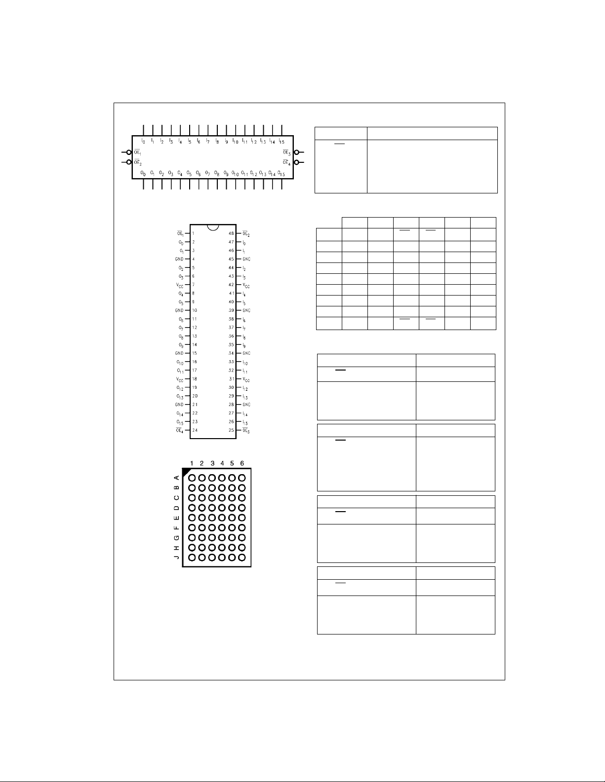
Logic Symbol
74ALVC162244
Connection Diagrams
Pin Assignment for TSSOP
Pin Assignment for FBGA
Pin Descriptions
Pin Names Description
I
O
OE
n
0–I15
0–O15
Output Enable Input (Active LOW)
Inputs
Outputs
NC No Connect
FBGA Pin Assignments
123456
A O
B O
C O
D O
E O
F O
G O
H O
J O
NC OE1OE2NC I
0
O1NC NC I
2
O3V
4
6
8
10
12O11VCCVCCI11
14O13
15
CCVCCI3
O5GND GND I
O7GND GND I
O9GND GND I
NC NC I
NC OE4OE3NC I
Truth Tables
Inputs Outputs
OE
1
LL L
LH H
HX Z
OE
2
LL L
LH H
HX Z
I0–I
3
Inputs Outputs
I4–I
7
1
5
7
9
13I14
O0–O
O4–O
0
I
2
I
4
I
6
I
8
I
10
I
12
15
3
7
(Top Thru View)
www.fairchildsemi.com 2
Inputs Outputs
OE
3
I8–I
11
LL L
LH H
HX Z
Inputs Outputs
OE
4
I12–I
15
O12–O
LL L
LH H
HX Z
H = HIGH Voltage Level
L = LOW Voltage Level
X = Immaterial (HIGH or LOW, inputs may not float)
Z = High Impedance
O8–O
11
15
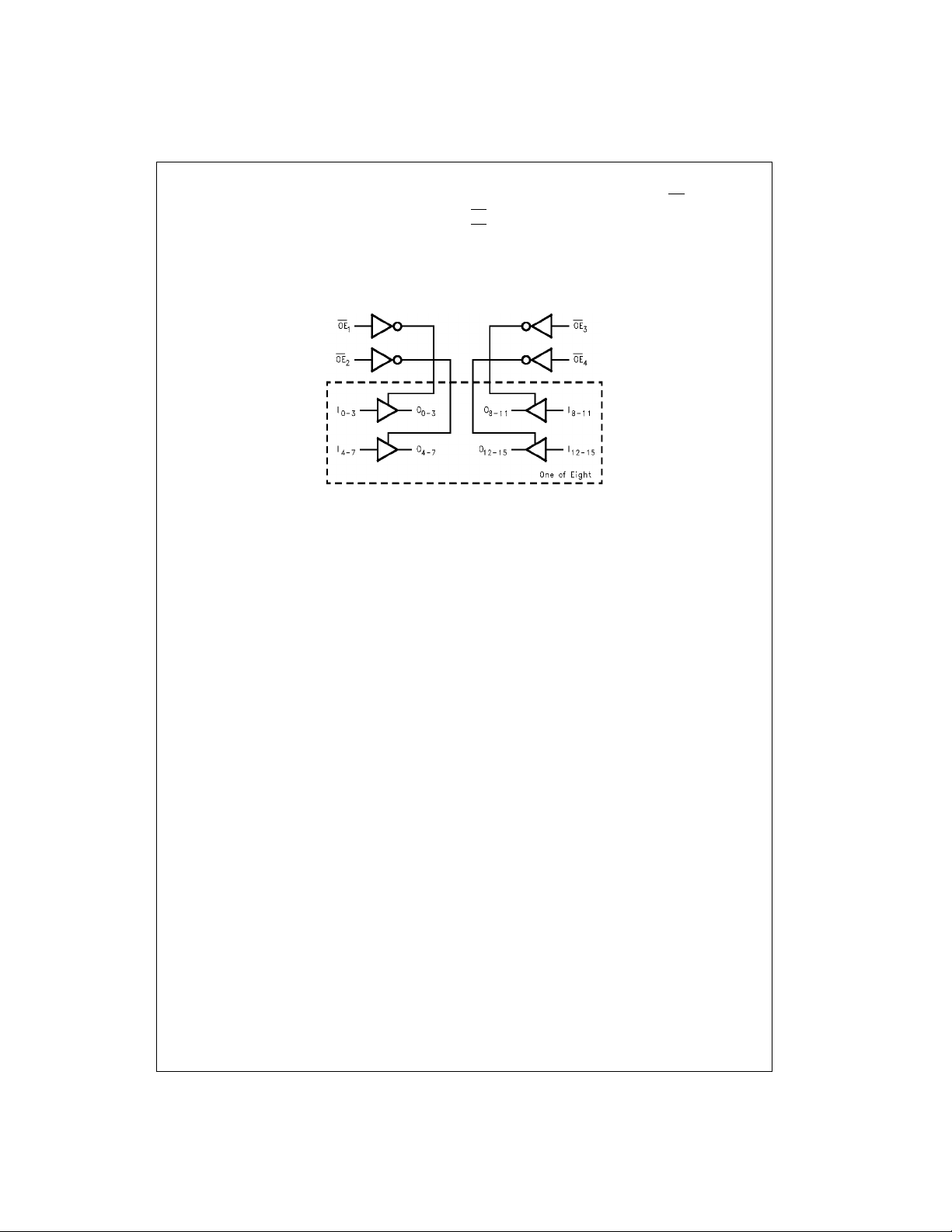
Functional Description
The 74ALVC162244 contains sixtee n non-inver ting buffers
with 3-STATE outputs. The device is nibble (4 bits) controlled with each nibble fun ction i ng ide ntically, but independent of each other. The control pins may be shorted
together to obtain full 16-bit op eration.The 3-STATE out-
Logic Diagram
puts are controlled by an Output Enable (OE
is LOW, the outputs are in the 2-state mode. W hen
OE
n
is HIGH, the standard outputs are in the high imped-
OE
n
ance mode but this does not interfere with entering new
data into the inputs.
) input. When
n
74ALVC162244
3 www.fairchildsemi.com
 Loading...