

Fairchild Semiconductor 74ALVC132 Datasheet
December 2001
Revised December 2001
74ALVC132
Low Voltage Quad 2-Input NAND Gate with
Schmitt Trigger Inputs and 3.6V Tolerant Inputs
and Outputs
74ALVC132 Low Voltage Quad 2-Input NAND Gate with Schmitt Trigger Inputs and 3.6V Tolerant Inputs and
Outputs
General Description
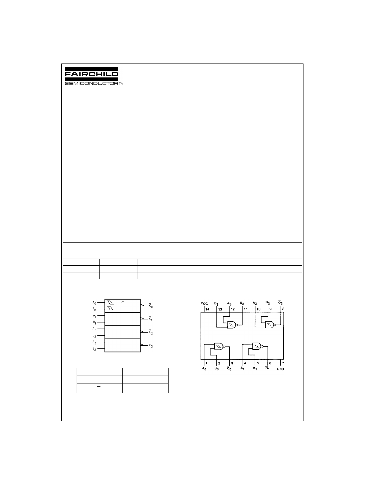
The ALVC132 contains four 2-input NAND gates with
Schmitt Trigger Inputs. The pin co nfiguration and funct ion
are the same as the ALVC00 except the inputs have hysteresis between the positive-going and negative-going
input thresholds. This hysteresis is useful for transforming
slowly switching input signals into sharply defined, jitterfree output signals. This product should be used where
noise margin greater than that of conventional gates is
required.
The ALVC132 is designed for low voltage (1.65V t o 3.6V)
V
applications with I/O compatibility up to 3.6V.
CC
This product is fabricated with an advanced CMOS tec hnology to achieve high-speed operation while maintaining
low CMOS power dissipation.
Features
■ 1.65V to 3.6V VCC supply operation
■ 3.6V tolerant inputs and outputs
■ t
PD
3.8 ns max for 3.0V to 3.6V V
4.6 ns max for 2.3V to 2.7V V
8.2 ns max for 1.65V to 1.95V V
■ Power-off high impedance inputs and outputs
■ Uses patented Quiet Series
circuitry
■ Latchup conforms to JEDEC JED78
■ ESD performance:
Human body model
Machine model
> 250V
CC
CC
CC
noise/EMI reduction
> 2000V
Ordering Code:
Order Number Package Number Package Description
74ALVC132M M14A 14-Lead Small Outline Integrated Circuit (SOIC), JEDEC MS-012, 0.150" Narrow
74ALVC132MTC MTC14 14-Lead Thin Shrink Small Outline Package (TSSOP), JEDEC MO-153, 4.4mm Wide
Devices also availab l e in Tape and Reel. Specify by appending su ffix let te r “X” to the ordering code.
Logic Diagram
Connection Diagram
Pin Descriptions
Pin Name Description
A
, B
n
n
O
n
Quiet Series is a tra demark of Fairchild Semiconductor Corp oration.
© 2001 Fairchild Semiconductor Corporation ds500720 www.fairchildsemi.com
Inputs
Outputs
Absolute Maximum Ratings(Note 1) Recommended Operating
Supply Voltage (VCC) −0.5V to +4.6V
DC Input Voltage (V
Output Voltage (V
74ALVC132
DC Input Diode Current (I
V
< 0V −50 mA
I
DC Output Diode Current (I
< 0V −50 mA
V
O
) −0.5V to 4.6V
I
) (Note 2) −0.5V to VCC +0.5V
O
)
IK
)
OK
DC Output Source/Sink Current
(I
) ±50 mA
OH/IOL
or GND Current per
DC V
CC
Supply Pin (I
Storage Temperature Range (T
or GND) ±100 mA
CC
) −65°C to +150°C
STG
Conditions
Power Supply
Operating 1.65V to 3.6V
Input Voltage (V
Output Voltage (VO) 0V to V
Free Air Operating Temperature (TA) −40°C to +85°C
Minimum Input Edge Rate (
= 0.8V to 2.0V, VCC = 3.0V 10 ns/V
V
IN
Note 1: The Absolute Maximum Ratings are those values beyond which
the safety of the d evice cannot be guaranteed. The device sh ould not be
operated at these limit s. The parametric values defin ed in the Electrical
Characteristics tables are not guaranteed at the Absolute Maximum Rat-
ings. The “Recommended Operating Conditions” table will define the conditions for actual device operation.
Absolute Maximum Rating must be observed.
Note 2: I
O
Note 3: Floating or unused inputs must be held HIGH or LOW.
(Note 3)
) 0V to V
I
∆t/∆V)
DC Electrical Characteristics
V
Symbol Parameter Conditions
Vt+ Positive Threshold 1.65 1.3
Vt− Negative Threshold 1.65 0.25
V
H
V
OH
V
OL
I
I
I
OZ
I
CC
∆I
Input Hysteresis 1.65 0.2 0.9
HIGH Level Output Voltage IOH = −100 µA 1.65 - 3.6 VCC - 0.2
LOW Level Output Voltage IOL = 100 µA 1.65 - 3.6 0.2
Input Leakage Current 0 ≤ VI ≤ 3.6V 3.6 ±5.0 µA
3-STATE Output Leakage 0 ≤ VO ≤ 3.6V 3.6 ±10 µA
Quiescent Supply Current VI = VCC or GND, IO = 0 3.6 40 µA
Increase in ICC per Input VIH = VCC − 0.6V 3 -3.6 750 µA
CC
IOH = −4 mA 1.65 1.2
I
= −6 mA 2.3 2
OH
= −12 mA 2.3 1.7
I
OH
IOH = −24 mA 3.0 2
IOL = 4 mA 1.65 0.45
IOL = 6 mA 2.3 0.4
IOL = 12mA 2.3 0.7
IOL = 24 mA 3 0.55
CC
(V)
2.3 1.6
3.0 2.0
3.6 2.2
2.3 0.5
3.0 0.7
3.6 0.8
2.3 0.3 1.0
3.0 0.3 1.2
3.6 0.3 1.2
2.7 2.2
3.0 2.4
2.7 0.4
Min Max Units
CC
CC
V
V
V
V
V
www.fairchildsemi.com 2
 Loading...