

Fairchild Semiconductor 74ACTQ843SPC, 74ACTQ843SCX, 74ACTQ843SC, 74ACTQ843CW Datasheet
March 1990
Revised December 1998
74ACTQ843 Quiet Series 9-Bit Transparent Latch with 3-STATE Outputs
© 1999 Fairchild Semiconductor Corporation DS010689.prf www.fairchildsemi.com
74ACTQ843
Quiet Series 9-Bit Transparent Latch
with 3-STATE Outputs
General Description
The ACTQ843 bus interface latch is de signed to eli minate
the extra packages required to buffer existing latches and
provide extra data width for wider address/data paths. The
ACTQ843 utilizes Fairchild FACT Quiet Series technology to guarantee quiet output switching and improved
dynamic threshold performance. FACT Quiet Series features GTO output control and undershoot corrector in
addition to a split ground bus for superior performance.
Features
■ Guaranteed simultaneous switching noise level and
dynamic threshold performance
■ Guaranteed pin-to-pin skew AC performance
■ Inputs and outputs on opposite sides of package for
easy interface with microprocessors
■ Improved latch-up immunity
■ Outputs source/sink 24 mA
■ ACTQ843 has TTL-compatible inputs
■ Functionally and pin-compatible to AMD’s AM29843
■ 3-STATE outputs for bus interfacing
Ordering Code:
Device also available in Tape and Reel. Specify by appendin g s uf f ix let t er “X” to the ordering co de.
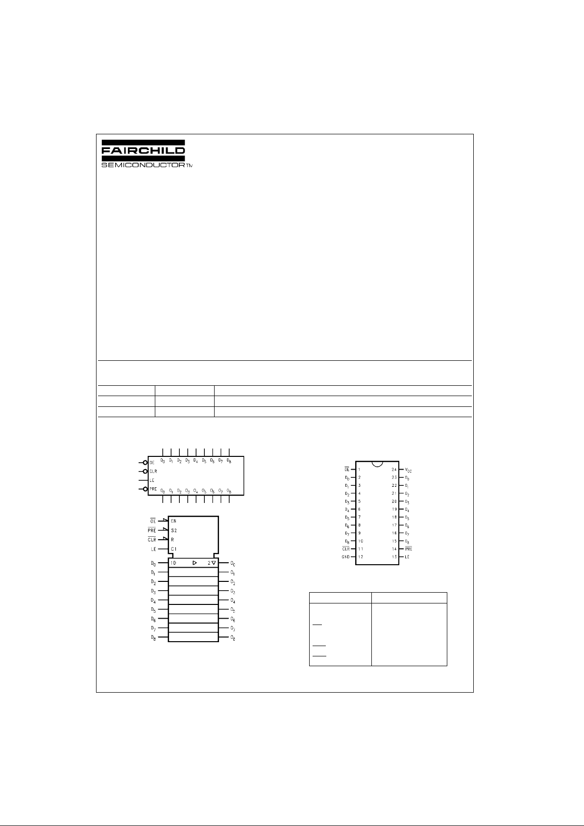
Logic Symbols Connection Diagram
Pin Assignment f or DIP and SOIC
Pin Descriptions
FACT, Quiet Series, FACT Quiet Series and GTO are trademarks of Fairchild Semiconductor Co rporation.
Order Number Package Number Package Description
74ACTQ843SC M24B 24-Lead Small Outline Integrated Circuit (SOIC), JEDEC MS-013, 0.300” Wide Body
74ACTQ843SPC N24C 24-Lead Plastic Dual-In-Line Package (PDIP), JEDEC MS-100, 0.300” Wide
Pin Names Description
D
0–D8
Data Inputs
O
0–O8
Data Outputs
OE
Output Enable
LE Latch Enable
CLR
Clear
PRE
Preset
www.fairchildsemi.com 2
74ACTQ843
Functional Description
The ACTQ843 consists of nine D-type latches with 3STATE outputs. The flip-flops appear transparent to the
data when Latch Enable (LE) is HIGH. This allows asynchronous operation, as the output transition follows the
data in transition. On t he LE HIGH-to-LOW transition, th e
data that meets the setup ti mes is latched. Data appea rs
on the bus when the Output Enable (OE
) is LOW. When
OE
is HIGH, the bus output is i n t he h igh i mpe da nce state.
In addition to the LE and OE
pins, the ACTQ843 has a
Clear (CLR
) pin and a Preset (PRE) pin. These pins are
ideal for parity bus interfacing in high performance systems. When CLR
is LOW, the outputs are LOW if OE is
LOW. When CLR
is HIGH, data can be entere d into the
latch. When PRE
is LOW, the outputs are HIGH if OE is
LOW. Preset overrides CLR
.
Function Table
H = HIGH Voltage Level
L = LOW V oltage Level
X = Immaterial
Z = High Impedance
NC = No Change
Logic Diagram
Inputs Internal Outputs Function
CLR
PRE OE LE D Q O
HHHHL L Z High Z
HHHHH H Z High Z
H H H L X NC Z Latched
H H L H L L L Transparent
H H L H H H H Transparent
H H L L X NC NC Latched
H L L X X H H Preset
L H L X X L L Clear
LLLXX H H Preset
L H H L X L Z Clear/High Z
HLHLX H Z Preset/High Z
3 www.fairchildsemi.com
74ACTQ843
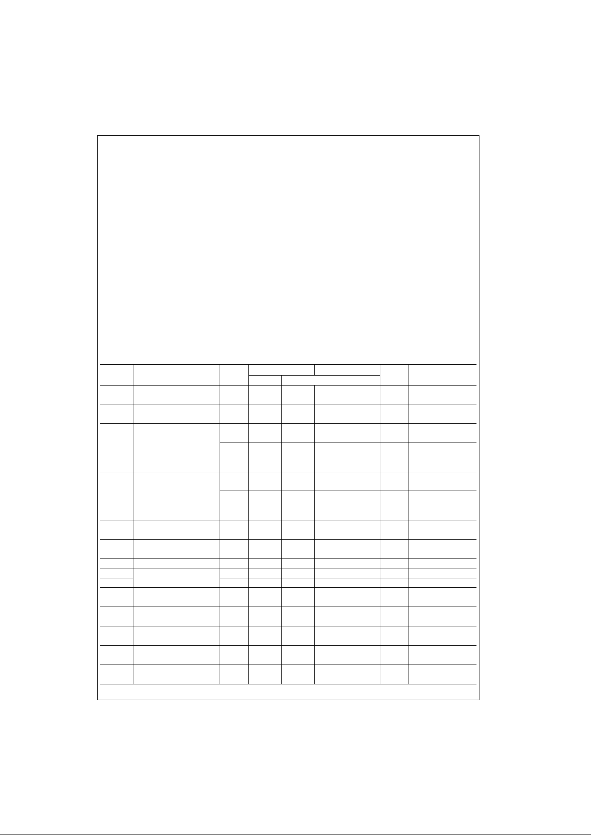
Absolute Maximum Ratings(Note 1)
Recommended Operating
Conditions
Note 1: Absolute maximum ratings are those values beyond which damage
to the device may occur. The databook specifications should be met, without exception, to ensure that the system design is reliable over its power
supply, temperature, and output/in put loading variables. Fairchild does n ot
recommend operat ion of FACT circuits outside databook specifications.
DC Electrical Characteristics
Supply Voltage (VCC) −0.5V to +7.0V
DC Input Diode Current (I
IK
)
V
I
= −0.5V −20 mA
V
I
= VCC + 0.5V +20 mA
DC Input Voltage (V
I
) −0.5V to VCC + 0.5V
DC Output Diode Current (I
OK
)
V
O
= −0.5V −20 mA
V
O
= VCC + 0.5V +20 mA
DC Output Voltage (V
O
) −0.5V to VCC + 0.5V
DC Output Source
or Sink Current (I
O
) ±50 mA
DC V
CC
or Ground Current
per Output Pin (I
CC
or I
GND
) ±50 mA
Storage Temperature (T
STG
) −65°C to +150°C
DC Latch-Up Source
or Sink Current ± 300 mA
Junction Temperature (T
J
)
PDIP 140°C
Supply Voltage (V
CC
) 4.5V to 5.5V
Input Voltage (V
I
) 0V to V
CC
Output Voltage (VO) 0V to V
CC
Operating Temperature (TA) −40°C to +85°C
Minimum Input Edge Rate ∆V/∆t 125 mV/ns
V
IN
from 0.8V to 2.0V
V
CC
@ 4.5V, 5.5V
Symbol Parameter
V
CC
TA = +25°C TA = −40°C to +85°C
Units Conditions
(V) Typ Guaranteed Limits
V
IH
Minimum HIGH Level 4.5 1.5 2.0 2.0 V V
OUT
= 0.1V
Input Voltage 5.5 1.5 2.0 2.0 or VCC − 0.1V
V
IL
Maximum LOW Level 4.5 1.5 0.8 0.8 V V
OUT
= 0.1V
Input Voltage 5.5 1.5 0.8 0.8 or VCC − 0.1V
V
OH
Minimum HIGH Level 4.5 4.49 4.4 4.4 V I
OUT
= −50 µA
Output Voltage 5.5 5.49 5.4 5.4
VIN = VIL or V
IH
4.5 3.86 3.76 V IOH = 24 mA
5.5 4.86 4.76 I
OH
= 24 mA (Note 2)
V
OL
Maximum LOW Level 4.5 0.001 0.1 0.1 V I
OUT
= 50 µA
Output Voltage 5.5 0.001 0.1 0.1
VIN = VIL or V
IH
4.5 0.36 0.44 V IOL = 24 mA
5.5 0.36 0.44 IOL = 24 mA (Note 2)
I
IN
Maximum Input 5.5 ± 0.1 ± 1.0 µAVI = VCC, GND
Leakage Current
I
OZ
Maximum 3-STATE 5.5 ± 0.5 ± 5.0 µAVI = VIL, V
IH
Leakage Current VO = VCC, GND
I
CCT
Maximum ICC/Input 5.5 0.6 1.5 mA VI = VCC − 2.1V
I
OLD
Minimum Dynamic 5.5 75 mA V
OLD
= 1.65V Max
I
OHD
Output Current (Note 3) 5.5 −75 mA V
OHD
= 3.85V Min
I
CC
Maximum Quiescent 5.5 8.0 80.0 µAVIN = V
CC
Supply Current or GND
V
OLP
Quiet Output 5.0 1.1 1.5 V Figure 1, Figure 2
Maximum Dynamic V
OL
(Note 4)(Note 5)
V
OLV
Quiet Output 5.0 −0.6 −1.2 V Figure 1, Figure 2
Minimum Dynamic V
OL
(Note 4)(Note 5)
V
IHD
Minimum HIGH Level 5.0 1.9 2.0 V (Note 4)(Note 6)
Dynamic Input Voltage
V
ILD
Maximum LOW Level 5.0 1.2 0.8 V (Note 4)(Note 6)
Dynamic Input Voltage
 Loading...