Fairchild Semiconductor 74ABT899CSCX, 74ABT899CSC, 74ABT899CQCX, 74ABT899CQC, 74ABT899CMSAX Datasheet
...
November 1992
Revised January 1999
74ABT899 9-Bit Latchable Transceiver with Parity Generator/Checker
© 1999 Fairchild Semiconductor Corporation DS011509.prf www.fairchildsemi.com
74ABT899
9-Bit Latchable Transceiver
with Parity Generator/Checker
General Description
The ABT899 is a 9-bit to 9- bit par ity transcei ver with transparent latches. The d evice can operate as a feed-through
transceiver or it can generate/ check parity from the 8-bit
data busses in either direction.
The ABT899 features inde pende nt la tch ena bles for the Ato-B direction and the B-to-A direction, a select pin for
ODD/EVEN
parity, and separate error signal output pins for
checking parity.
Features
■ Latchable transceiver with output sink of 64 mA
■ Option to select generate parity and check or
“feed-through” data/parity in directions A-to-B or B-to-A
■ Independent latch enables for A-to-B and B-to-A
directions
■ Select pin for ODD/EVEN
parity
■ ERRA
and ERRB output pins for parity checking
■ Ability to simultaneously generate and check parity
■ May be used in systems applications in place of the
543 and 280
■ May be used in system applications in place of the
657 and 373 (no need to change T/R
to check parity)
■ Guaranteed output skew
■ Guaranteed multiple output switching specifications
■ Output switching specified for both 50 pF and
250 pF loads
■ Guaranteed simultaneous switching noise level and
dynamic threshold performance
■ Guaranteed latchup protection
■ High impedance glitch free bus loading during entire
power up and power down cycle
■ Nondestructive hot insertion capability
■ Disable time less than enable time to avoid bus
contention
Ordering Code:
Devices also available in Tape and Reel. Specify by appending suffix letter “X” to the ordering code.
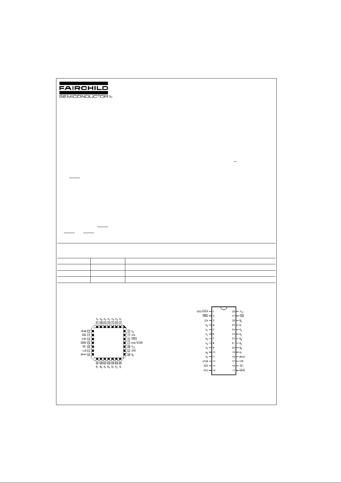
Connection Diagrams
Pin Assignment
for PLCC
Pin Assignment f or
SOIC and SSOP
Order Number Package Number Package Description
74ABT899CSC M28B 28-Lead Small Outline Integrated Circuit (SOIC), MS-013, 0.300” Wide Body
74ABT899CMSA MSA28 28-Lead Shrink Small Outline Package (SSOP), EIAJ TYPE II, 5.3mm Wide
74ABT899CQC V28A 28-Lead Plastic Lead Chip Carrier (PLCC), JEDEC MO-047, 0.450” Square
www.fairchildsemi.com 2
74ABT899
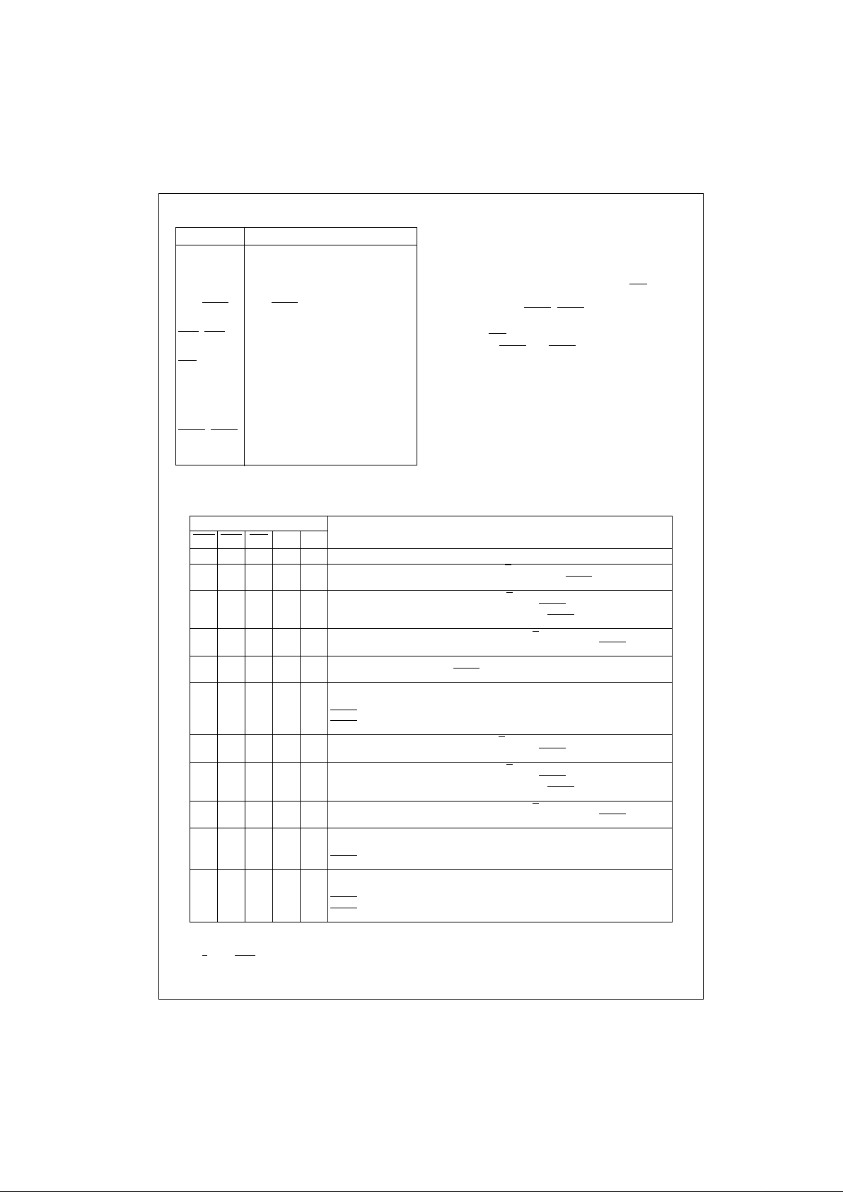
Pin Descriptions Functional Description
The ABT899 has three prin cipa l mode s of op erat ion w hich
are outlined below. These modes apply t o both the A- to-B
and B-to-A directions.
• Bus A (B) communicates to Bus B ( A), parity is generated and passed on to the B (A) Bus as BPAR (APAR). If
LEB (LEA) is HIGH and t he Mode Sele ct ( SEL
) is LOW,
the parity generated from B[0:7] (A[0:7]) can be checked
and monitored by ERRB
(ERRA).
• Bus A (B) communicates to Bus B (A) in a feed-through
mode if SEL
is HIGH. Parity is still generated and
checked as ERRA
and ERRB in the feed-th rough mo de
(can be used as an interru pt to signal a data/parity bit
error to the CPU).
• Independent Latch E nables (LEA and LEB) allow oth er
permutations of generating/checking (see Function
Table below).
Function Table
H = HIGH Voltage Level
L = LOW V oltage Level
X = Immaterial
Note 1: O/E
= ODD/EVEN
Pin Names Descriptions
A
0–A7
A Bus Data Inputs/Data Outputs
B
0–B7
B Bus Data Inputs/Data Outputs
APAR, BPAR A and B Bus Parity Inputs/Outputs
ODD/EVEN
ODD/EVEN Parity Select,
Active LOW fo r EVEN Parity
GBA
, GAB Output Enables for A or B Bus,
Active LOW
SEL
Select Pin for Feed-Through or
Generate Mode, LOW for Generate
Mode
LEA, LEB Latch Enables for A and B Latches,
HIGH for Transparent Mode
ERRA
, ERRB Error Signals for Checking Generated
Parity with Parity In, LOW if Error
Occurs
Inputs Operation
GAB
GBA SEL LEA LEB
H H X X X Busses A and B are 3-STATE.
H L L L H Generates parity from B[0:7] based on O/E
(Note 1). Generated parity → APAR.
Generated parity checked against BPAR and output as ERRB
.
HLLHH
Generates parity from B[0:7] based on O/E
. Generated parity → APAR. Gener-
ated parity checked against BPAR and output as ERRB
. Generated parity also
fed back through the A latch for generate/check as ERRA
.
HLLXL
Generates parity from B latch data based on O/E
. Generated parity → APAR.
Generated parity checked against latched BPAR and output as ERRB
.
H L H X H BPAR/B[0:7] → APAR/A0:7] Feed-through mode. Generated parity checked
against BPAR and output as ERRB
.
H L H H H BPAR/B[0:7] → APAR/A[0:7]
Feed-through mode. Generated parity checked against BPAR and output as
ERRB
. Generated parity also fed back through the A latch for generate/check as
ERRA
.
LHLHL
Generates parity for A[0:7] based on O/E
. Generated parity → BPAR. Gener-
ated parity checked against APAR and output as ERRA
.
LHLHH
Generates parity from A[0:7] based on O/E
. Generated parity → BPAR. Gener-
ated parity checked against APAR and output as ERRA
. Generated parity also
fed back through the B latch for generate/check as ERRB
.
LHLLX
Generates parity from A latch data based on O/E
. Generated parity → BPAR.
Generated parity checked against latched APAR and output as ERRA
.
L H H H L AP AR/A[0:7] → BPAR/B[0:7]
Feed-through mode. Generated parity checked against APAR and output as
ERRA
.
L H H H H APAR/A[0:7] → BPAR/B[0:7]
Feed-through mode. Generated parity checked against APAR and output as
ERRA
. Generated parity also fed back through the B latch for generate/check as
ERRB
.
3 www.fairchildsemi.com
74ABT899
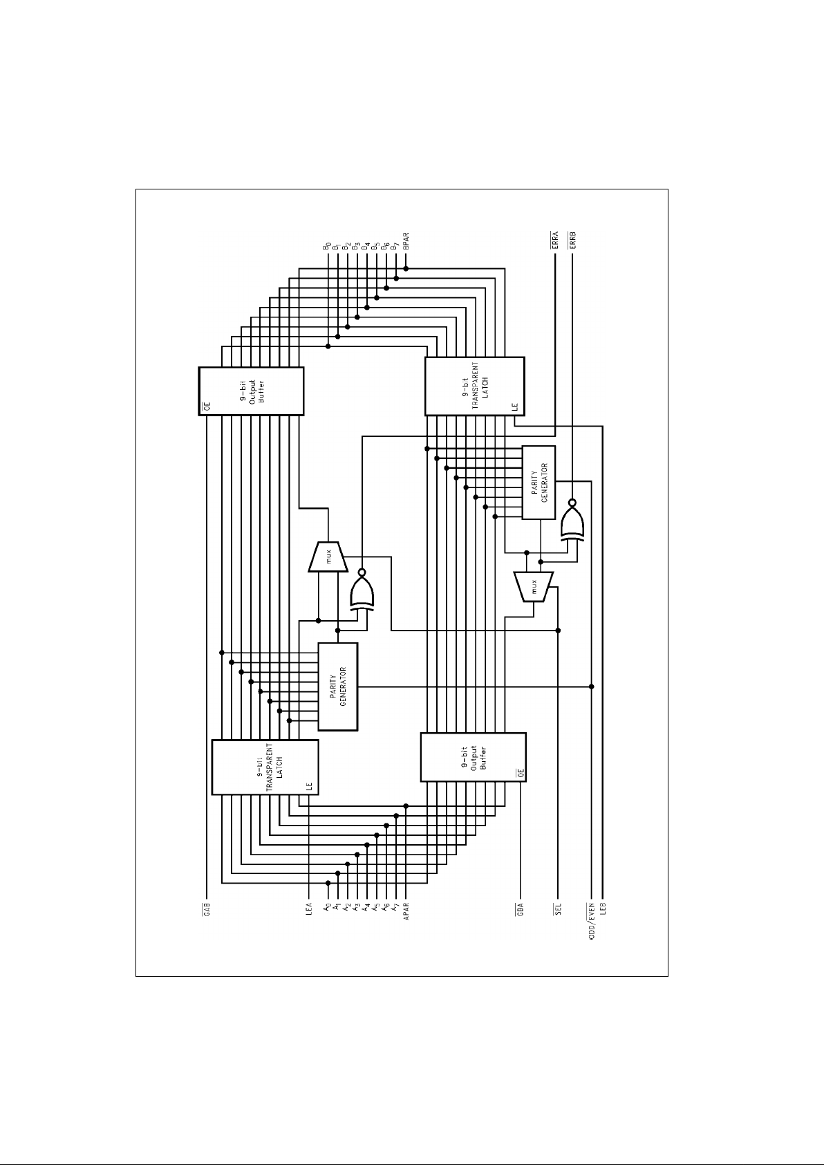
Functional Block Diagram
www.fairchildsemi.com 4
74ABT899
Absolute Maximum Ratings(Note 2)
Recommended Operating
Conditions
Note 2: Absolute maximum ratings are values beyond which the device
may be damaged or have its useful life impaired. Functional operation
under these conditi ons is not implied.
Note 3: Either voltage limit or current limit is s uf f ic ient to protect inputs.
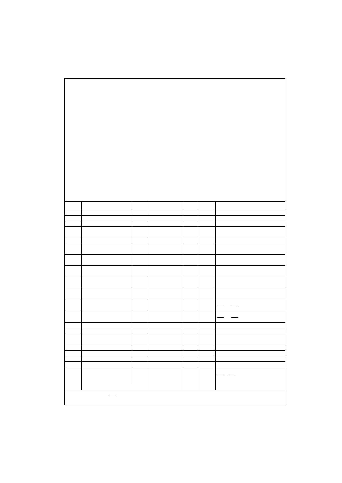
DC Electrical Characteristics
Note 4: Guaranteed, but not tested.
Note 5: Add 3.75 mA for each ERR
LOW.
Storage Temperature −65°C to +150°C
Ambient Temperature under Bias −55°C to +125°C
Junction Temperature under Bias
Plastic −55°C to +150°C
V
CC
Pin Potential to
Ground Pin −0.5V to +7.0V
Input Voltage (Note 3) −0.5V to +7.0V
Input Current (Note 3) −30 mA to +5.0 mA
Voltage Applied to Any Output
in the Disable or PowerOff State −0.5V to +5.5V
in the HIGH State −0.5V to V
CC
Current Applied to Output
in LOW State (Max)
twice therated I
OL
(mA)
DC Latchup Source Current −500 mA
Over Voltage Latchup (I/O) 10V
Free Air Ambient Temperature −40°C to +85°C
Supply Voltage +4.5V to +5.5V
Minimum Input Edge Rate (∆V/∆t)
Data Input 50 mV/ns
Enable Input 20 mV/ns
Symbol Parameter Min Typ Max Units
V
CC
Conditions
V
IH
Input HIGH Voltage 2.0 V Recognized HIGH Signal
V
IL
Input LOW Voltage 0.8 V Recognized LOW Signal
V
CD
Input Clamp Diode Voltage −1.2 V Min IIN = −18 mA (Non I/O Pins)
V
OH
Output HIGH 2.5 V Min IOH = −3 mA, (An, Bn, APAR, BPAR)
Voltage 2.0 IOH = −32 mA, (An, Bn, APAR, BPAR)
V
OL
Output LOW Voltage 0.55 V Min IOL = 64 mA, (An, Bn, APAR, BPAR)
V
ID
Input Leakage Te st 4.75 V 0.0 IID = 1.9 µA, (Non-I/O Pins)
All Other Pins Grounded
I
IH
Input HIGH Current 5 µAMaxVIN = 2.7V (Non-I/O Pins) (Note 4)
VIN = VCC (Non-I/O Pins)
I
BVI
Input HIGH Current 7 µAMaxVIN = 7.0V (Non-I/O Pins)
Breakdown Test
I
BVIT
Input HIGH Current 100 µAMaxVIN = 5.5V (An, Bn, APAR, BPAR)
Breakdown Test (I/O)
I
IL
Input LOW Current −5 µAMaxVIN = 0.5V (Non-I/O Pins) (Note 4)
VIN = 0.0V (Non-I/O Pins)
IIH + I
OZH
Output Leakage Current 50 µA 0V–5.5V V
OUT
= 2.7V (An, Bn);
GAB and GBA = 2.0V
IIL + I
OZL
Output Leakage Current −50 µA 0V–5.5V V
OUT
= 0.5V (An, Bn);
GAB and GBA = 2.0V
I
OS
Output Short-Circuit Current −100 −275 mA Max V
OUT
= 0V (An, Bn, APAR, BPAR)
I
CEX
Output HIGH Leakage Current 50 µAMaxV
OUT
= VCC (An, Bn, APAR, BPAR)
I
ZZ
Bus Drainage T est 100 µA0.0VV
OUT
= 5.5V (An, Bn, APAR, BPAR);
All Others GND
I
CCH
Power Supply Current 250 µA Max All Outputs HIGH
I
CCL
Power Supply Current 34 mA Max All Outputs LOW, ERRA/B = HIGH (Note 5)
I
CCZ
Power Supply Current 250 µA Max Outputs 3-STATE All Others at VCC or GND
I
CCT
Additional ICC/Input 2.5 mA Max VI = VCC − 2.1V All Others at VCC or GND
I
CCD
Dynamic ICC: No Load 0.4 mA/MHz Max Outputs Open
(Note 4)
GAB or GBA = GND, LE = HIGH
Non-I/O = GND or V
CC
One bit toggling, 50% duty cycle
5 www.fairchildsemi.com
74ABT899
DC Electrical Characteristics
(PLCC package)
Note 6: Max number of ou t puts defined as (n). n − 1 data inputs are driven 0V to 3V. One output at LOW. Guaranteed, but not tested.
Note 7: Max number o f dat a inp uts (n) switchi ng. n − 1 in put s switchin g 0V t o 3V. Input-under-tes t switchi ng: 3 V to th resh old (V
ILD
), 0V to threshold (V
IHD
).
Guaranteed, but not tested.
Note 8: Max number of ou t puts defined as (n). n − 1 data inpu t s a re driven 0V to 3V. One output HIGH. Guaranteed, but not tested.
AC Electrical Characteristics
(SOIC and PLCC Package)
Symbol Parameter Min Typ Max Units
V
CC
Conditions
CL = 50 pF, RL = 500Ω
V
OLP
Quiet Output Maximum Dynamic V
OL
0.8 1.1 V 5.0 TA = 25°C (Note 6)
V
OLV
Quiet Output Minimum Dynamic V
OL
−1.3 −0.8 V 5.0 TA = 25°C (Note 6)
V
OHV
Minimum HIGH Level Dynamic Output Voltage 2.5 3.0 V 5.0 TA = 25°C (Note 8)
V
IHD
Minimum HIGH Level Dynamic Input Voltage 2.2 1.8 V 5.0 TA = 25°C (Note 7)
V
ILD
Maximum LOW Level Dynamic Input Voltage 0.8 0.5 V 5.0 TA = 25°C (Note 7)
Symbol Parameter
TA = +25°CT
A
= −40°C to +85°C
Units
VCC = +5.0V VCC = 4.5V–5.5V
CL = 50 pF CL = 50 pF
Min Typ Max Min Max
t
PLH
Propagation Delay 1.5 3.0 4.8 1.5 4.8 ns
t
PHL
An, to B
n
1.5 3.5 4.8 1.5 4.8
t
PLH
Propagation Delay 2.5 5.9 9.2 2.5 9.2 ns
t
PHL
An, Bn to BPAR, APAR 2.5 5.8 9.2 2.5 9.2
t
PLH
Propagation Delay 2.5 5.4 8.5 2.5 8.5 ns
t
PHL
An, Bn to ERRA, ERRB
2.5 5.4 8.5 2.5 8.5
t
PLH
Propagation Delay 1.5 3.7 6.0 1.5 6.0 ns
t
PHL
APAR, BPAR to ERRA, ERRB
1.5 3.7 6.0 1.5 6.0
t
PLH
Propagation Delay 2.0 4.4 6.9 2.0 6.9 ns
t
PHL
ODD/EVEN to APAR, BPAR 2.0 4.4 6.9 2.0 6.9
t
PLH
Propagation Delay 1.8 4.0 6.0 1.8 6.0 ns
t
PHL
ODD/EVEN to ERRA, ERRB
1.8 4.0 6.0 1.8 6.0
t
PLH
Propagation Delay 1.5 3.8 6.0 1.5 6.0 ns
t
PHL
SEL to APAR, BPAR 1.5 3.8 6.0 1.5 6.0
t
PLH
Propagation Delay 1.5 3.2 4.6 1.5 4.6 ns
t
PHL
LEA, LEB to Bn, A
n
1.5 3.2 4.6 1.5 4.6
t
PLH
Propagation Delay 2.5 5.9 8.8 2.5 8.8
nst
PHL
LEA, LEB to BPAR, APAR 2.5 5.7 8.8 2.5 8.8
Generate Mode
t
PLH
Propagation Delay 1.5 3.6 5.1 1.5 5.1 ns
t
PHL
LEA, LEB to BPAR, APAR, 1.5 3.6 5.1 1.5 5.1
Feed Thru Mode
t
PLH
Propagation Delay 1.6 5.4 8.4 1.6 8.4 ns
t
PHL
LEA, LEB to ERRA, ERRB
1.6 5.4 8.4 1.6 8.4
t
PZH
Output Enable Time 1.5 3.6 6.0 1.5 6.0 ns
t
PZL
GBA or GAB to An,
1.5 3.4 6.0 1.5 6.0
APAR or Bn, BPAR
t
PHZ
Output Disable Time 1.0 4.0 6.0 1.0 6.0 ns
t
PLZ
GBA or GAB to An,
1.0 3.3 6.0 1.0 6.0
APAR or Bn, BPAR
t
PLHtPHL
Propagation Delay 1.5 3.3 5.4 1.5 5.4 ns
APAR to BPAR, BPAR to APAR 1.5 3.8 5.4 1.5 5.4
 Loading...