

Fairchild Semiconductor 74ABT646CMSA, 74ABT646CSPC, 74ABT646CSCX, 74ABT646CSC, 74ABT646CMTCX Datasheet
...
© 1999 Fairchild Semiconductor Corporation DS010978 www.fairchildsemi.com
April 1992
Revised November 1999
74ABT646 Octal Transceivers and Registers with 3-STATE Outputs
74ABT646
Octal Transceivers and Registers with 3-STATE Outputs
General Description
The ABT646 consists of bus transceiver circuits with 3STATE , D-type flip -flops, and c ontrol circu itry arranged for
multiplexed transmission of da ta directly from the input bus
or from the internal registers. Data on the A or B bus will be
clocked into the registers as the appropriate clock pin goes
to a high logic level. Control OE
and direction pins are pr ovided to control the tr ansceiver function. In the tran sceiver
mode, data present at the high impedance port may be
stored in either the A or the B register or in both. The select
controls can multiplex stored and real-time (transparent
mode) data. The direction control determines which bus
will receive data when the enable control OE
is Active
LOW. In the isolation mode (control OE
HIGH), A data may
be stored in the B register a nd/or B data may be stored in
the A regis ter.
Features
■ Independent registers for A and B buses
■ Multiplexed real-time and stored data
■ A and B output sink capability of 64 mA, source capabil-
ity of 32 mA
■ Guaranteed output skew
■ Guaranteed multiple output switching specifications
■ Output switching sp ecified for both 50 pF and 250 pF
loads
■ Guaranteed simultaneous switching noise level and
dynamic threshold performan ce
■ Guarante ed latchup protection
■ High impedance glitch free bus loading during entire
power up and power down cycle
■ Nondestructive hot insertion capability
Ordering Code:
Device also available in Tape and Reel. Specify by appending s uffix let te r “X” to the ordering code.
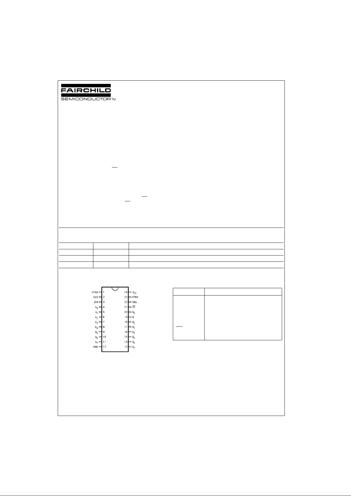
Connection Diagram Pin Descriptions
Order Number Package Number Package Description
74ABT646CSC M24B 24-Lead Small Outline Integrated Circuit (SOIC), JEDEC MS-153, 4.4mm Wide
74ABT646CMSA MSA24 24-Lead Shrink Small Outline Package (SSOP), EIAJ TYPE II, 5.3mm Wide
74ABT646CMTC MTC24 24-Lead Thin Shrink Small Outline Package (TSSOP), JEDEC MO-153, 4.4mm Wide
Pin Names Description
A
0–A7
Data Register A Inputs/3-STATE Outputs
B
0–B7
Data Register B Inputs/3-STATE Outputs
CPAB, CPBA Clock Pulse Inputs
SAB, SBA Select Inputs
OE
Output Enable Input
DIR Direction Control Input
www.fairchildsemi.com 2
74ABT646
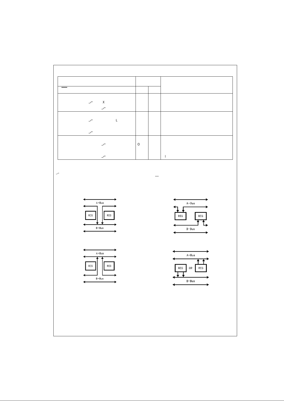
Truth Table
H = HIGH Voltage Level
L = LOW Voltage Level
X = Immaterial
= LOW-to-HIGH Transition
Note 1: The data output functions may be enabled or dis abled by various signals at the OE
and DIR inputs. Data input functions are always enabled;
i.e., data at the bus pins will be stored on every LOW-to-HIGH transition of the appropriate clock inputs.
Real Time Transfer
A-Bus to B-Bus
FIGURE 1.
Real Time Transfer
B-Bus to A-Bus
FIGURE 2.
Storage from
Bus to Register
FIGURE 3.
Transfer from
Register to Bus
FIGURE 4.
Inputs Data I/O
(Note 1)
Function
OE
DIR CPAB CPBA SAB SBA A0–A7 B0–B
7
H X H or L H or L X X Isolation
H X
X X X Input Input Clock An Data into A Register
H X X
X X Clock Bn Data into B Register
L H X X L X A
n
to Bn—Real Time (Transparent Mode)
L H
X L X Input Output Clock An Data into A Register
L H H or L X H X A Register to B
n
(Stored Mode)
L H
X H X Clock An Data into A Register and Output to B
n
L L X X X L Bn to An—Real Time (Transparent Mode)
L L X
X L Output Input Clock Bn Data into B Register
L L X H or L X H B Register to A
n
(Stored Mode)
L L X
X H Clock Bn Data into B Register and Output to A
n
3 www.fairchildsemi.com
74ABT646
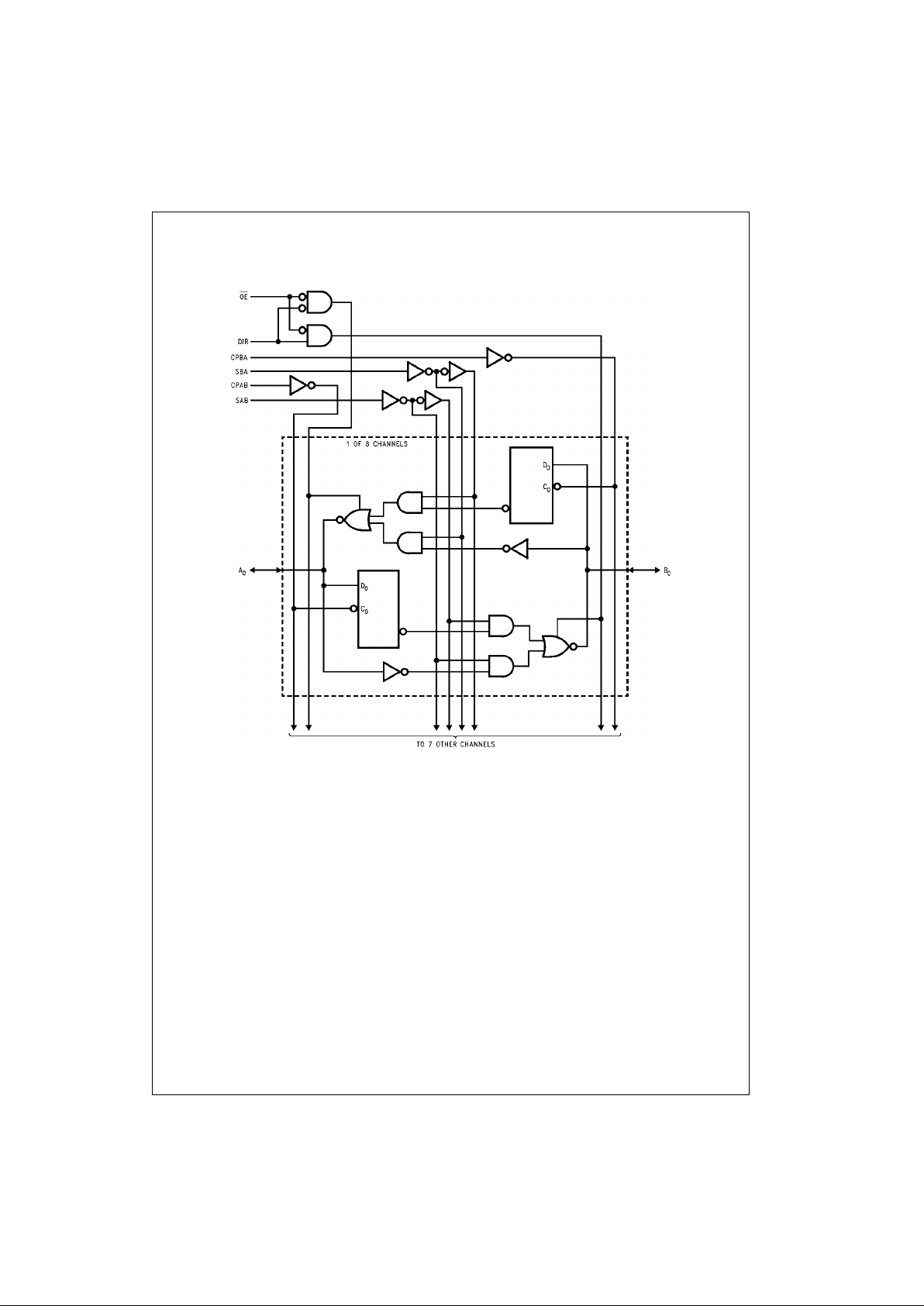
Logic Diagram
Please note that this diagram is provided only for the understanding of logic operations and should not be used to estimate propagation delays.
 Loading...