

Fairchild Semiconductor 74ABT573CSJX, 74ABT573CSJ, 74ABT573CSCX, 74ABT573CSC, 74ABT573CPC Datasheet
...
© 1999 Fairchild Semiconductor Corporation DS011548 www.fairchildsemi.com
January 1993
Revised November 1999
74ABT573 Octal D-Type Latch with 3-STATE Outputs
74ABT573
Octal D-Type Latch with 3-STATE Outputs
General Description
The ABT573 is an octal latch with buffered com mon Latch
Enable (LE) and buffered common Output Enable (OE
)
inputs.
This device is functionally iden tical to the ABT373 bu t has
broadside pinouts.
Features
■ Inputs and outputs on opposit e sides of package allow
easy interface with microprocessors
■ Useful as input or output port for microprocessors
■ Functionally identical to ABT373
■ 3-STATE outputs for bus interfacing
■ Output sink capability of 64 mA, source capability of
32 mA
■ Guaranteed output skew
■ Guaranteed multiple output switching specifications
■ Output switching sp ecified for both 50 pF and 250 pF
loads
■ Guaranteed simultaneous switching, noise level and
dynamic threshold performan ce
■ Guarante ed latchup protection
■ High impedance glitch-free bus loading during entire
power up and power down
■ Nondestructive hot insertion capability
Ordering Code:
Devices also availab le in Tape and Reel. Specify by appending th e s uffix let t er “X” to the ordering code.
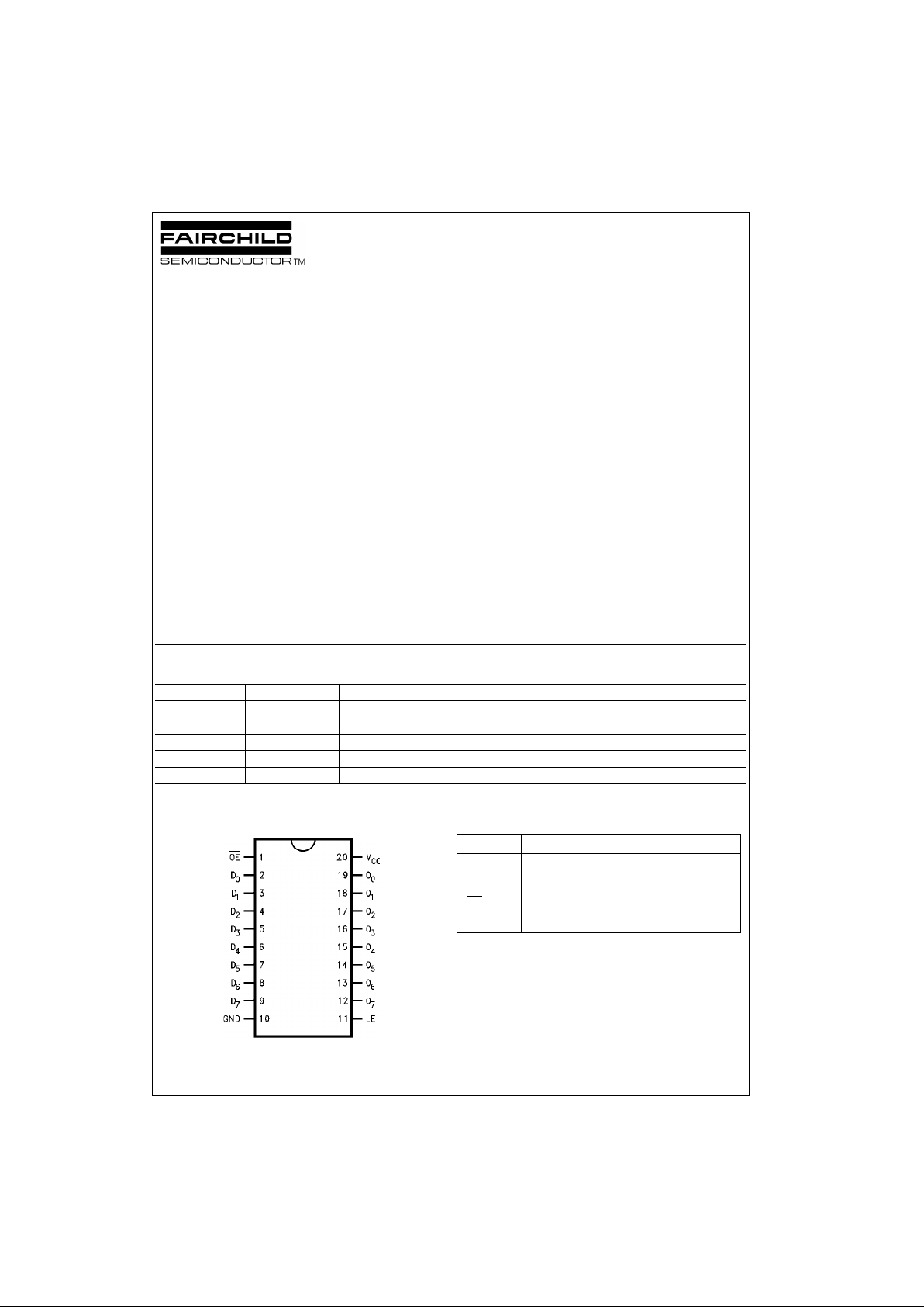
Connection Diagram Pin Descriptions
Order Number Package Number Package Description
74ABT573CSC M20B 20-Lead Small Outline Integrated Circuit (SOIC), JEDEC MS-013, 0.300” Wide Body
74ABT573CSJ M20D 20-Lead Small Outline Package (SOP), EIAJ TYPE II, 5.3mm Wide
74ABT573CMSA MSA20 20-Lead Shrink Small Outline Package (SSOP), EIAJ TYPE II, 5.3mm Wide
74ABT573CMTC MTC20 20-Lead Thin Shrink Small Outline Package (TSSOP), JEDEC MO-153, 4.4mm Wide
74ABT573CPC N20A 20-Lead Plastic Dual-In-L ine (P DIP ), JED EC MS-01, 0.3 00” Wide
Pin Names Descriptions
D
0–D7
Data Inputs
LE Latch Enable Input (Active HIGH)
OE
3-STATE Output Enable Input (Active LOW)
O
0–O7
3-STATE Latch Outputs
www.fairchildsemi.com 2
74ABT573
Functional Description
The ABT573 contains eig ht D-type latches with 3-STATE
output buffers. When the La tch Enab le ( LE) inpu t is HI GH,
data on the D
n
inputs enters the latches. In this conditio n
the latches are transparent, i.e., a latch output will change
state each time its D input ch anges. Whe n LE is L OW the
latches store the information that was present on th e D
inputs a setup time preceding the HIGH-to-LOW transitio n
of LE. The 3-STATE buffers are controlled by th e Output
Enable (OE
) input. When OE is LOW, the buffers are in the
bi-state mode. When OE
is HIGH the buffers are in the high
impedance mode but this does not interfere with entering
new data into the latches.
Function Table
H = HIGH Voltage Level
L = LOW Voltage Level
X = Immaterial
O
0
= Value stored from previous clock cycle
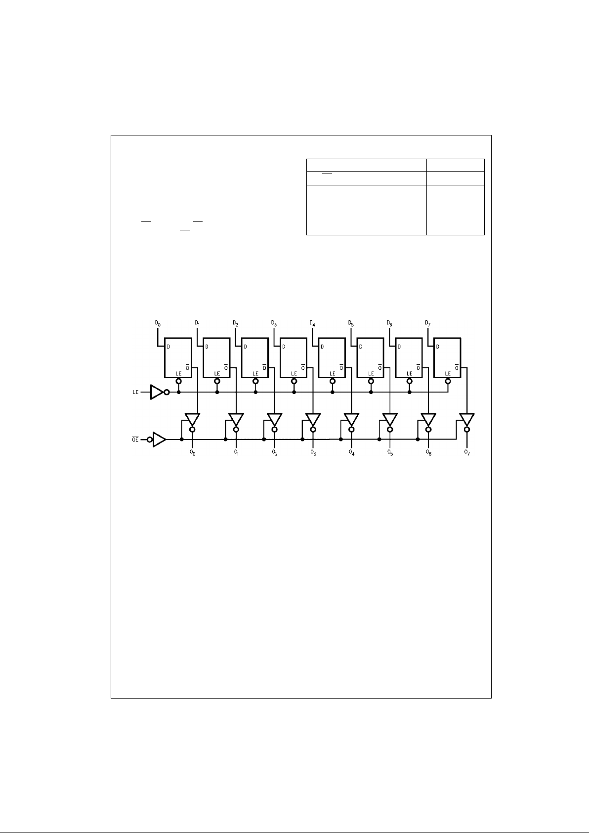
Logic Diagram
Please note that this diagram is provided only for the understanding of logic operations and should not be used to estimate propagation delays.
Inputs Outputs
OE LE D O
LHH H
LHL L
LLX O
0
HXX Z
3 www.fairchildsemi.com
74ABT573
Absolute Maximum Ratings(Note 1) Recommended Operating
Conditions
Note 1: Absolute maximum ratings are values beyond which the device
may be damaged or have its useful life impaired . Functional operation
under these conditions is not implied.
Note 2: Either voltage lim it or c urrent limit is sufficient to protect inputs.
DC Electrical Characteristics
Note 3: For 8 bits toggling, I
CCD
< 0.8 mA/MHz.
Note 4: Guaranteed but not tested.
Storage Temperature −65°C to +150°C
Ambient Temperature under Bias −55°C to +125°C
Junction Temperature under Bias −55°C to +150°C
V
CC
Pin Potential to Ground Pin −0.5V to +7.0V
Input Voltage (Note 2) −0.5V to +7.0V
Input Current (Note 2) −30 mA to +5.0 mA
Voltage Applied to Any Output
in the Disabled or
Power-Off State −0.5V to +5.5V
in the HIGH State −0.5V to V
CC
Current Applied to Output
in LOW State (Max) Twice the rated I
OL
(mA)
DC Latchup Source Current −500 mA
Over Voltage Latchup (I/O) 10V
Free Air Ambient Temperature −40°C to +85°C
Supply Voltage +4.5V to +5.5V
Minimum Input Edge Rate (∆V/∆t)
Data Input 50 mV/ns
Enable Input 20 mV/ns
Symbol Parameter Min Typ Max Units
V
CC
Conditions
V
IH
Input HIGH Voltage 2.0 V Recognized HIGH Signal
V
IL
Input LOW Voltage 0.8 V Recognized LOW Signal
V
CD
Input Clamp Diode Voltage −1.2 V Min IIN = −18 mA
V
OH
Output HIGH Voltage 2.5
VMin
IOH = −3 mA
2.0 IOH = −32 mA
V
OL
Output LOW Voltage 0.55 V Min IOL = 64 mA
I
IH
Input HIGH Current 1
µAMax
VIN = 2.7V (Note 4)
1V
IN
= V
CC
I
BVI
Input HIGH Current
7 µAMaxVIN = 7.0V
Breakdown Test
I
IL
Input LOW Current −1
µAMax
VIN = 0.5V (Note 4)
−1V
IN
= 0.0V
V
ID
Input Leakage Test 4.75 V 0.0 IID = 1.9 µA
All Other Pins Grounded
I
OZH
Output Leakage Current 10 µA0 − 5.5V
V
OUT
= 2.7V; OE = 2.0V
I
OZL
Output Leakage Current −10 µA0 − 5.5V
V
OUT
= 0.5V; OE = 2.0V
I
OS
Output Short-Circuit Current −100 −275 mA Max V
OUT
= 0.0V
I
CEX
Output HIGH Leakage Current 50 µAMaxV
OUT
= V
CC
I
ZZ
Bus Drainage Test 100 µA0.0V
OUT
= 5.5V; All Others GND
I
CCH
Power Supply Current 50 µA Max All Outputs HIGH
I
CCL
Power Supply Current 30 mA Max All Outputs LOW
I
CCZ
Power Supply Current
50 µAMax
OE = V
CC
All Others at VCC or GND
I
CCT
Additional ICC/Input Outputs Enabled 2.5 mA VI = VCC − 2.1V
Outputs 3-STATE 2.5 mA Max Enable Input VI = VCC − 2.1V
Outputs 3-STATE 2.5 mA Data Input VI = VCC − 2.1V
All Others at VCC or GND
I
CCD
Dynamic I
CC
No Load mA/ Max Outputs Open
(Note 4) 0.12
MHz
OE = GND, LE = VCC (Note 3)
One Bit Toggling, 50% Duty Cycle
www.fairchildsemi.com 4
74ABT573
DC Electrical Characteristics
Note 5: Max number of output s d ef ined as (n). n − 1 data inputs are driven 0V to 3V. One output at LOW. Guaranteed, but not t es t ed.
Note 6: Max number of output s d ef ined as (n). n − 1 data inputs are driven 0V to 3V. One output HIGH. Guaranteed, but not tested.
Note 7: Max number of data input s (n ) swit chin g. n − 1 inputs switching 0V to 3V. Input-under-test switching: 3V to threshold (V
ILD
), 0V to threshold (V
IHD
).
Guaranteed, but not tested.
AC Electrical Characteristics
(SOIC and SSOP Package)
AC Operating Requirements
(SOIC and SSOP Package)
Symbol Parameter Min Typ Max Units
V
CC
Conditions
CL = 50 pF, RL = 500Ω
V
OLP
Quiet Output Maximum Dynamic V
OL
0.7 1.0 V 5.0 TA = 25°C (Note 5)
V
OLV
Quiet Output Minimum Dynamic V
OL
−1.5 −1.2 V 5.0 TA = 25°C (Note 5)
V
OHV
Minimum HIGH Level Dynamic Output Voltage 2.5 3.0 V 5.0 TA = 25°C (Note 6)
V
IHD
Minimum HIGH Level Dynamic Input Voltage 2.2 1.8 V 5.0 TA = 25°C (Note 7)
V
ILD
Maximum LOW Level Dynamic Input Voltage 1.0 0.7 V 5.0 TA = 25°C (Note 7)
Symbol Parameter
T
A
= +25°CT
A
= −40°C to +85°C
Units
V
CC
= +5.0V VCC = 4.5V to 5.5V
CL = 50 pF CL = 50 pF
Min Typ Max Min Max
t
PLH
Propagation Delay 1.9 2.7 4.5 1.9 4.5
ns
t
PHL
Dn to O
n
1.9 2.8 4.5 1.9 4.5
t
PLH
Propagation Delay 2.0 3.1 5.0 2.0 5.0
ns
t
PHL
LE to O
n
2.0 3.0 5.0 2.0 5.0
t
PZH
Output Enable Time 1.5 3.1 5.3 1.5 5.3
ns
t
PZL
1.5 3.1 5.3 1.5 5.3
t
PHZ
Output Disable Time 2.0 3.6 5.4 2.0 5.4
ns
t
PLZ
Time 2.0 3.4 5.4 2.0 5.4
Symbol Parameter
TA = +25°CT
A
= −40°C to +85°C
Units
VCC = +5.0V VCC = 4.5V to 5.5V
CL = 50 pF CL = 50 pF
Min Typ Max Min Max
f
TOGGLE
Max Toggle Frequency 100 MHz
tS(H) Set Time, HIGH 1.5 1.5
ns
t
S
(L) or LOW Dn to LE 1.5 1.5
t
H
(H) Hold Time, HIGH 1.0 1.0
ns
tH(L) or LOW Dn to LE 1.0 1.0
tW(H) Pulse Width,
3.0 3.0 ns
LE HIGH
 Loading...