

Fairchild Semiconductor 74ABT543CSPC, 74ABT543CSCX, 74ABT543CSC, 74ABT543CMTCX, 74ABT543CMTC Datasheet
...
November 1992
Revised January 1999
74ABT543 Octal Registered Transceiver with 3-STATE Outputs
© 1999 Fairchild Semiconductor Corporation DS011508.prf www.fairchildsemi.com
74ABT543
Octal Registered Transceiver with 3-STATE Outputs
General Description
The ABT543 octal transceiver conta ins two sets of D-type
latches for temporary storage of data flowing in either
direction. Separate Latch Enable and Output Enabl e inputs
are provided for each register to permit indep endent control of inputting and outputt ing in either direction of data
flow.
Features
■ Back-to-back registers for storage
■ Bidirectional data path
■ A and B outputs have current sourcing capability of 32
mA and current sinking capability of 64 mA
■ Separate controls for data flow in each direction
■ Guaranteed output skew
■ Guaranteed multiple output switching specifications
■ Output switching specified for both 5 0 pF and 250 pF
loads
■ Guaranteed simultaneous switching noise level and
dynamic threshold performance
■ Guaranteed latchup protection
■ High impedance glitch free bus loading during entire
power up and power down cycle
■ Nondestructive hot insertion capability
Ordering Code:
Device also available in Tape and Reel. Specify by appendin g s uf f ix let t er “X” to the ordering co de.
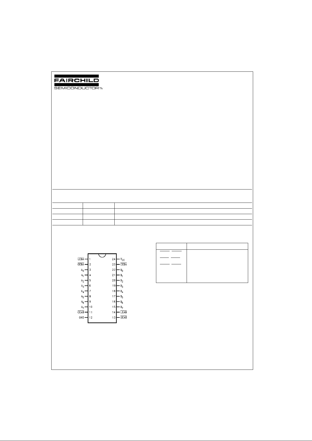
Connection Diagram
Pin Assignment for
SOIC, SSOP and TSSOP
Pin Descriptions
Order Number Package Number Package Description
74ABT543CSC M24B 24-Lead Small Outline Integrated Circuit (SOIC), JEDEC MS-013, 0.300” Wide Body
74ABT543CMSA MSA24 24-Lead Shrink Small Outline Package (SSOP), EIAJ TYPE II, 5.3mm Wide
74ABT543CMTC MTC24 24-Lead Thin Shrink Small Outline Package (TSSOP), JEDEC MO-153, 4.4mm Wide
Pin Names Description
OEAB
, OEBA Output Enable Inputs
LEAB
, LEBA Latch Enable Inputs
CEAB
, CEBA Chip Enable Inputs
A
0–A7
Side A Inputs or 3-STATE Outputs
B
0–B7
Side B Inputs or 3-STATE Outputs
www.fairchildsemi.com 2
74ABT543
Functional Description
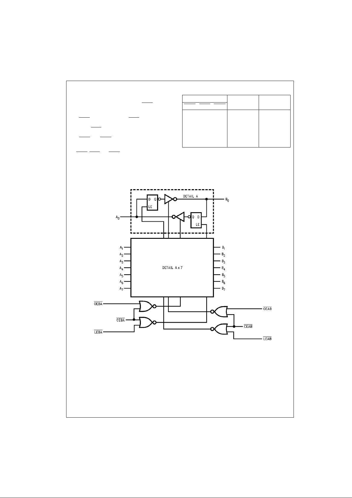
The ABT543 contains two sets of D-type latches, with separate input and output co ntr ols for each. For data flow fro m
A to B, for example, the A to B Enable (CEAB
) input must
be low in order to enter data from the A Port or take da ta
from the B Port as i ndicated in the Da ta I/O Contr ol Table.
With CEAB
low, a low signal on (LEAB) input makes the A
to B latches transparent; a subse quent low to high transition of the LEAB
line puts the A latches in the storage
mode and their outputs no longer change with the A inputs.
With CEAB
and OEAB both low, the B output buffers are
active and reflect the data present on the output of the A
latches. Control of data flow from B to A is similar, but using
the CEBA
, LEBA and OEBA.
Data I/O Control Table
H = HIGH Voltage Level
L = LOW Voltage Level
X = Immaterial
Logic Diagram
Inputs Latch Status Output Buffers
CEAB
LEAB OEAB
H X X Latched HIGH Z
X H X Latched —
L L X Transparent —
X X H — HIGH Z
L X L — Driving
3 www.fairchildsemi.com
74ABT543
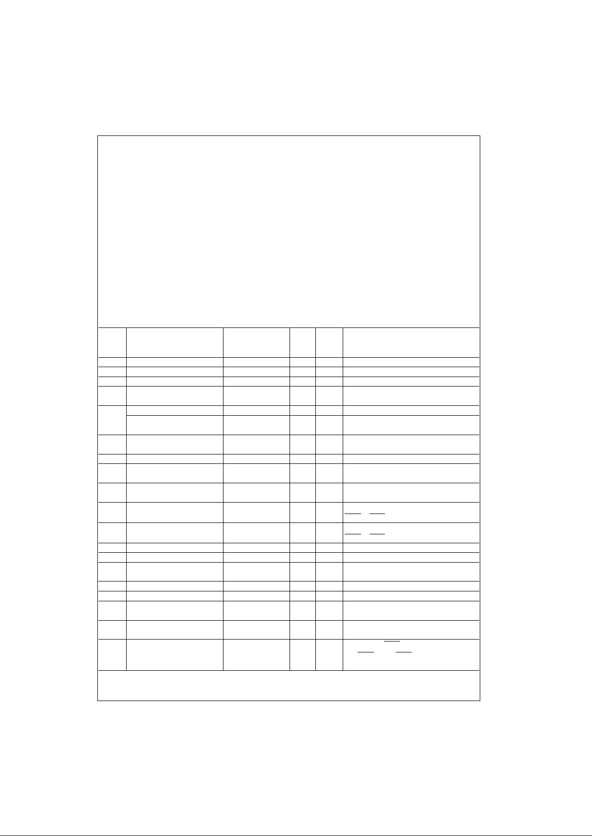
Absolute Maximum Ratings(Note 1)
Recommended Operating
Conditions
Note 1: Absolute maximum ratings are values beyond which the device
may be damaged or have its useful life impaired. Functional operation
under these condit ions is not implied.
Note 2: Either voltage limit or current limi t is s uf f ic ient to protect inputs.
DC Electrical Characteristics
Note 3: Guaranteed but not tested.
Note 4: For 8-bit toggling. I
CCD
< 1.4 mA/MHz.
Note 5: Guaranteed, but not tested.
Storage Temperature −65°C to +150°C
Ambient Temperature under Bias −55°C to +125°C
Junction Tem perature under Bias −55°C to +150°C
V
CC
Pin Potential to
Ground Pin −0.5V to +7.0V
Input Voltage (Note 2) −0.5V to +7.0V
Input Current (Note 2) −30 mA to +5.0 mA
Voltage Applied to Any Output
in the Disable or Power-Off State −0.5V to +5.5V
in the HIGH State −0.5V to V
CC
Current Applied to Output
in LOW State (Max)
twice the rated I
OL
(mA)
DC Latchup Source Current −500 mA
Over Voltage Latchup (I/O) 10V
Free Air Ambient Temperature −40°C to +85°C
Supply Voltage +4.5V to +5.5V
Minimum Input Edge Rate (∆V/∆t)
Data Input 50 mV/ns
Enable Input 20 mV/ns
Clock Input 100 mV/ns
Symbol Parameter Min Typ Max Units
V
CC
Conditions
V
IH
Input HIGH Voltage 2.0 V Recognized HIGH Signal
V
IL
Input LOW Voltage 0.8 V Recognized LOW Signal
V
CD
Input Clamp Diode Voltage −1.2 V IIN = −18 mA (Non I/O Pins)
V
OH
Output HIGH Voltage 2.5 IOH = −3 mA, (An, Bn)
2.0 IOH = −32 mA, (An, Bn)
V
OL
Output LOW Voltage 0.55 V Min IOL = 64 mA, (An, Bn)
V
ID
Input Leakage Test 4.75 V 0.0 IID = 1.9 µA, (Non-I/O Pins)
All Other Pins Grounded
I
IH
Input HIGH Current 1 µAMaxVIN = 2.7V (Non-I/O Pins) (Note 3)
1V
IN
= VCC (Non-I/O Pins)
I
BVI
Input HIGH Current Breakdown Test 7 µAMaxVIN = 7.0V (Non-I/O Pins)
I
BVIT
Input HIGH Current 100 µAMaxVIN = 5.5V (An, Bn)
Breakdown Test (I/O)
I
IL
Input LOW Current −1 µAMaxVIN = 0.5V (Non-I/O Pins) (Note 3)
−1V
IN
= 0.0V (Non-I/O Pins)
IIH+ I
OZH
Output Leakage Current 10 µA 0V–5.5V V
OUT
= 2.7V (An, Bn);
OEAB or CEAB = 2V
IIL + I
OZL
Output Leakage Current −10 µA 0V–5.5V V
OUT
= 0.5V (An, Bn);
OEAB or CEAB = 2V
I
OS
Output Short-Circuit Current −100 −275 mA Max V
OUT
= 0V (An, Bn)
I
CEX
Output HIGH Leakage Current 50 µAMaxV
OUT
= VCC (An, Bn)
I
ZZ
Bus Drainage Test 100 µA0.0VV
OUT
= 5.5V (An, Bn);
All Others GND
I
CCLH
Power Supply Current 50 µA Max All Outputs HIGH
I
CCL
Power Supply Current 30 mA Max All Outputs LOW
I
CCZ
Power Supply Current 50 µA Max Outputs 3-STATE
All Others at VCC or GND
I
CCT
Additional ICC/Input 2.5 mA Max VI = VCC − 2.1V
All Others at VCC or GND
I
CCD
Dynamic I
CC
No Load
Outputs Open, CEAB
(Note 5) 0.18 mA/MHz Max
and OEAB = GND, CEBA = VCC, One Bit Toggling,
50% Duty Cycle, (Note 4)
 Loading...