

Fairchild Semiconductor 74ABT2952CSPC, 74ABT2952CSCX, 74ABT2952CSC, 74ABT2952CMTCX, 74ABT2952CMTC Datasheet
...
© 1999 Fairchild Semiconductor Corporation DS010969 www.fairchildsemi.com
January 1992
Revised November 1999
74ABT2952 Octal Registered Transceiver
74ABT2952
Octal Registered Transceiver
General Description
The ABT2952 is an octal registered transce iver. Two 8-bit
back to back registe rs stor e dat a flowi ng in both direct ions
between two bidirectional buses. Separate clock, clock
enable and 3-STATE output enable signals are provided for
each register. The output pins are guaranteed to source 32
mA and to sink 64 mA.
Features
■ Separate clock, clock enable and 3-STATE output
enable provided for each register
■ A and B output sink capability of 64 mA source capability
of 32 mA
■ Guaranteed output skew
■ Guaranteed multiple output switching specifications
■ Output switching specifie d for both 50 pF and 250 pF
loads
■ Guaranteed simultaneous switching noise level and
dynamic threshold performan ce
■ Guaranteed latchup protection
■ High impedance glitch free bus loading during entire
power up and power down cycle
■ Nondestructive hot insertion capability
Ordering Code:
Device also available in Tape and Reel. Specify by appending the suffix letter “X” to the ordering code.
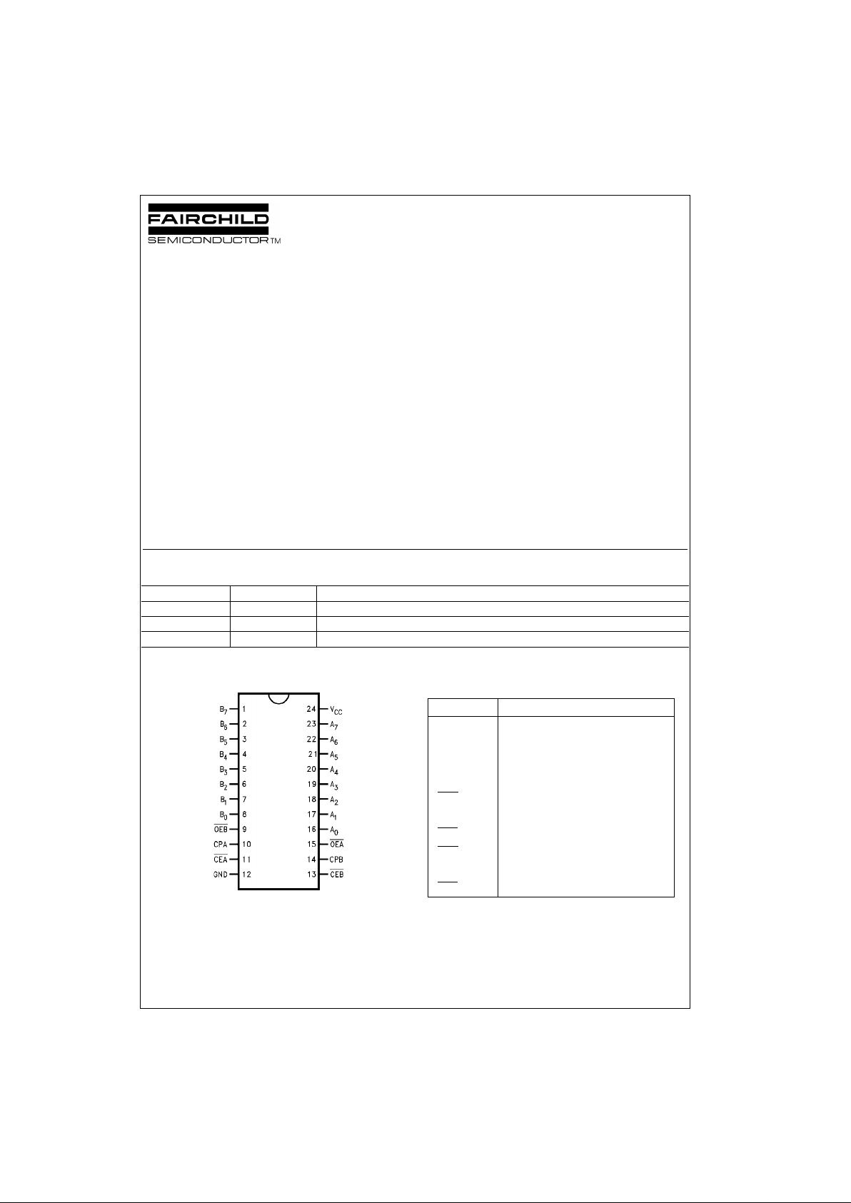
Connection Diagram Pin Descriptions
Order Number Package Numb er Package Description
74ABT2952CSC M24B 24-Lead Small Outline Integrated Circuit (SOIC), JEDEC MS-013, 0.300” Wide Body
74ABT2952CMSA MSA24 24-Lead Shrink Small Outline Package (SSOP), EIAJ TYPE II, 5.3mm Wide
74ABT2952CMTC MTC24 24-Lead Thin Shrink Small Outline Package (TSSOP), JEDEC MO-153, 4.4mm Wide
Pin Names Description
A
0–A7
A-Register Inputs/B-Register
3-STATE Outputs
B
0–B7
B-Register Inputs/A-Register
3-STATE Outputs
OEA
Output Enable A-Register
CPA A-Register Clock
CEA
A-Register Clock Enable
OEB
Output Enable B-Register
CPB B-Register Clock
CEB
B-Register Clock Enable
www.fairchildsemi.com 2
74ABT2952
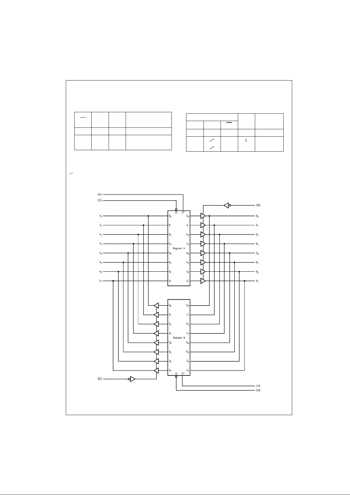
Truth Table
Output Control
Register Function Table (Applies to A or B Register)
H = HIGH Voltage Level
L = LOW Voltage Level
X = Immaterial
Z = HIGH Impedance
= LOW-to-HIGH Transition
NC = No Change
Block Diagram
OE
Internal
Output Function
Q
H X Z Disable Outputs
LLLEnable Outputs
LHH
Inputs Internal
Function
DCPCEQ
X X H NC Hold Data
L
L L Load Data
H
LH
3 www.fairchildsemi.com
74ABT2952
Absolute Maximum Ratings(Note 1) Recommended Operating
Conditions
Note 1: Absolute maximum ratings are values beyond which the device
may be damaged or have its useful life impaired . Functional operation
under these conditions is not implied.
Note 2: Either voltage lim it or c urrent limit is sufficient to pro te c t in puts.
DC Electrical Characteristics
Note 3: Guaranteed, but not tested.
Note 4: For 8-bit toggling, I
CCD
< 1.4 mA/MHz.
Storage Temperature −65°C to +150°C
Ambient Temperature under Bias −55°C to +125°C
Junction Temperature under Bias −55°C to +150°C
V
CC
Pin Potential to Ground Pin −0.5V to +7.0V
Input Voltage (Note 2) −0.5V to +7.0V
Input Current (Note 2) −30 mA to +5.0 mA
Voltage Applied to Any Output
in the Disable or
Power-Off State −0.5V to +5.5V
in the HIGH State −0.5V to V
CC
Current Applied to Output
in LOW State (Max) twice the rated I
OL
(mA)
DC Latchup Source Current −500 mA
Over Voltage Latchup (I/O) 10V
Free Air Ambient Temperature −40°C to +85°C
Supply Voltage +4.5V to +5.5V
Minimum Input Edge Rate (∆V/∆t)
Data Input 50 mV/ns
Enable Input 20 mV/ns
Clock Input 100 mV/ns
Symbol Parameter Min Typ Max Units
V
CC
Conditions
V
IH
Input HIGH Voltage 2.0 V Recognized HIGH Signal
V
IL
Input LOW Voltage 0.8 V Recognized LOW Signal
V
CD
Input Clamp Diode Voltage −1.2 V Min IIN = −18 mA (Non I/O Pins)
V
OH
Output HIGH Voltage 2.5 IOH = −3 mA (An, Bn)
2.0 IOH = −32 mA (An, Bn)
V
OL
Output LOW Voltage 0.55 V Min IOL = 64 mA (An, Bn)
V
ID
Input Leakage Test 4.75 V 0.0 IID = 1.9 µA (Non-I/O Pins)
All Other Pins Grounded
I
IH
Input HIGH Current 1
µAMax
VIN = 2.7V (Non-I/O Pins) (Note 3)
1V
IN
= VCC (Non-I/O Pins)
I
BVI
Input HIGH Current Breakdown Test 7 µAMaxVIN = 7.0V (Non-I/O Pins)
I
BVIT
Input HIGH Current Breakdown Test (I/O) 100 µAMaxVIN = 5.5V (An, Bn)
I
IL
Input LOW Current −1
µAMax
VIN = 0.5V (Non-I/O Pins) (Note 3)
−1V
IN
= 0.0V (Non-I/O Pins)
I
IH
+ I
OZH
Output Leakage Current 10 µA0V–5.5V V
OUT
= 2.7V (An, Bn);
OEA
or OEB = 2.0V
I
IL
+ I
OZL
Output Leakage Current −10 µA0V–5.5V V
OUT
= 0.5V (An, Bn);
OEA
or OEB = 2.0V
I
OS
Output Short-Circuit Current −100 −275 mA Max V
OUT
= 0V (An, Bn)
I
CEX
Output HIGH Leakage Current 50 µAMaxV
OUT
= VCC (An, Bn)
I
ZZ
Bus Drainage Test 100 µA0.0VV
OUT
= 5.5V (An, Bn);
All Others GND
I
CCH
Power Supply Current 250 µA Max All Outputs HIGH
I
CCL
Power Supply Current 30 mA Max All Outputs LOW
I
CCZ
Power Supply Current 50 µA Max Outputs 3-STATE;
All Others GND
I
CCT
Additional ICC/Input 2.5 mA Max VI = VCC − 2.1V; All Others
at VCC or GND
I
CCD
Dynamic I
CC
No Load 0.18 mA/MHz Max Outputs Open
(Note 4)
OEA or OEB = GND,
Non-I/O = GND or V
CC
One Bit toggling, 50% duty cycle
(Note 4)
 Loading...