

Fairchild Semiconductor 74ABT2541CSCX, 74ABT2541CSC, 74ABT2541CPC, 74ABT2541CMTCX, 74ABT2541CMTC Datasheet
...
© 1999 Fairchild Semiconductor Corporation DS011502 www.fairchildsemi.com
September 1992
Revised November 1999
74ABT2541 Octal Buffer/Line Driver with 25Ω Series Resistors in the Outputs
74ABT2541
Octal Buffer/Line Driver with
25Ω Series Resistors in the Outputs
General Description
The ABT2541 is an octal buffer and line driver desig ned to
drive the capacitive inputs of MOS memory drivers,
address drivers, clock drivers, an d bus-oriented transmitters/receivers. Functionally identical to the ABT541.
The 25Ω series resist ors i n the outputs reduc e r inging a nd
eliminate the need for external resistors.
Features
■ Guaranteed output ske w
■ Guaranteed multiple output switching specifications
■ Output switching specified for both 50 pF and
250 pF loads
■ Guaranteed simultaneously switching noise level and
dynamic threshold performan ce
■ Guarante ed latchup protection
■ High impedance glitch free bus loading during entire
power up and power down cycle
■ Nondestructive hot insertion capability
■ Disable time less than enable time to avoid bus
contention
Ordering Code:
Devices also availab le in Tape and Reel. Specify by appending “X” to the ordering co de.
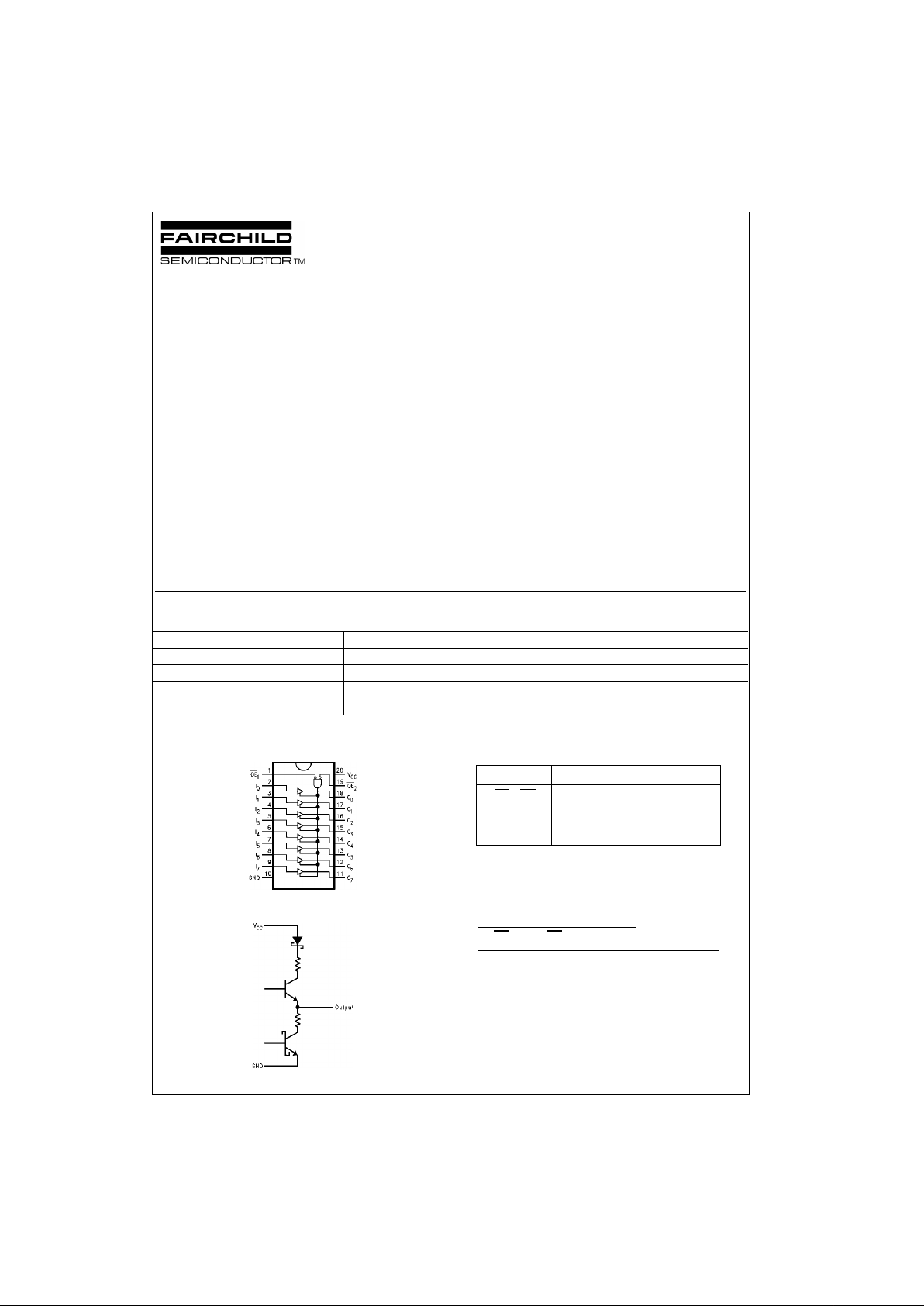
Connection Diagram
Schematic of Each Output
Pin Descriptions
Truth Table
H = HIGH Voltage Level
L = LOW Voltage Level
X = Immaterial
Z = High Impedance
Order Number Package Numb er Package Description
74ABT2541CSC M20B 20-Lead Small Outline Integrated Circuit (SOIC), JEDEC MS-013, 0.300” Wide Body
74ABT2541CSJ M20D 20-Lead Small Outline Package (SOP), EIAJ TYPE II, 5.3mm Wide
74ABT2541CMSA MSA20 20-Lead Shrink Small Outline Package (SSOP), EIAJ TYPE II, 5.3mm Wide
74ABT2541CMTC MTC20 20-Lead Thin Shrink Small Outline Package (TSSOP), JEDEC MO-153, 4.4mm Wide
Pin Names Description
OE
1
, OE2Output Enable Input (Active LOW)
I
0–I7
Inputs
O
0–O7
Outputs
Inputs
Outputs
OE
1
OE
2
I
L L H H
H X X Z
X H X Z
L L L L
www.fairchildsemi.com 2
74ABT2541
Absolute Maximum Ratings(Note 1) Recommended Operating
Conditions
Note 1: Absolute maximum ratings are values beyond which the device
may be damaged or have its useful life impaired. Functional operation
under these conditi ons is not implied.
Note 2: Either voltage lim it or c urrent limit is sufficient to prot ect inputs.
DC Electrical Characteristics
Note 3: Guaranteed, but not tested.
Note 4: For 8 bit toggling, I
CCD
< 0.8 mA/MHz.
Storage Temperature −65°C to +150°C
Ambient Temperature under Bias −55°C to +125°C
Junction Temperature under Bias −55°C to +150°C
V
CC
Pin Potential to Ground Pin −0.5V to +7.0V
Input Voltage (Note 2) −0.5V to +7.0V
Input Current (Note 2) −30 mA to +5.0 mA
Voltage Applied to Any Output
in the Disabled or
Power-Off State −0.5V to 5.5V
in the HIGH State −0.5V to V
CC
Current Applied to Output
in LOW State (Max) twice the rated I
OL
(mA)
DC Latchup Source Current −500 mA
Over Voltage Latchup (I/O) 10V
Free Air Ambient Temperature −40°C to +85°C
Supply Voltage +4.5V to +5.5V
Minimum Input Edge Rate (∆V/∆t)
Data Input 50 mV/ns
Enable Inpu t 20 mV/ns
Symbol Parameter Min Typ Max Units
V
CC
Conditions
V
IH
Input HIGH Voltage 2.0 V Recognized HIGH Signal
V
IL
Input LOW Voltage 0.8 V Recognized LOW Signal
V
CD
Input Clamp Diode Voltage −1.2 V Min IIN = −18 mA
V
OH
Output HIGH Voltage 2.5 V Min IOH = −3 mA
2.0 V Min IOH = −32 mA
V
OL
Output LOW Voltage 0.8 V Min IOL = 15 mA
I
IH
Input HIGH Current 1 µA MaxVIN = 2.7V (Note 3)
1V
IN
= V
CC
I
BVI
Input HIGH Current
7 µA MaxVIN = 7.0V
Breakdown Test
I
IL
Input LOW Current −1
µA Max
VIN = 0.5V (Note 3)
−1V
IN
= 0.0V
V
ID
Input Leakage Test 4.75 V 0.0 IID = 1.9 µA
All Other Pins Grounded
I
OZH
Output Leakage Current 10 µA 0 − 5.5V
V
OUT
= 2.7V; OEn = 2.0V
I
OZL
Output Leakage Current −10 µA 0 − 5.5V
V
OUT
= 0.5V; OEn = 2.0V
I
OS
Output Short-Circuit Current −100 −275 mA Max V
OUT
= 0.0V
I
CEX
Output High Leakage Current 50 µA MaxV
OUT
= V
CC
I
ZZ
Bus Drainage Test 100 µA 0.0V
OUT
= 5.5V; All Others GND
I
CCH
Power Supply Current 50 µA Max All Outputs HIGH
I
CCL
Power Supply Current 30 mA Max All Outputs LOW
I
CCZ
Power Supply Current
50 µA Max
OEn = VCC;
All Others at VCC or GND
I
CCT
Additional ICC/Input Outputs Enabled 2.5 mA VI = VCC − 2.1V
Outputs 3-STATE 2.5 mA Max Enable Input VI = VCC − 2.1V
Outputs 3-STATE 50 µA Data Input VI = VCC − 2.1V
All Others at VCC or GND
I
CCD
Dynamic I
CC
No Load mA/
Max
Outputs OPEN
(Note 4) 0.1
MHz
OEn = GND (Note 3)
One Bit Toggling, 50% Duty Cycle
3 www.fairchildsemi.com
74ABT2541
DC Electrical Characteristics
(SOIC Package)
Note 5: Max number of outputs def ined as (n). n-1 data inputs are driven 0V to 3V. One output at LOW. Guaranteed, but not tes te d.
Note 6: Max number of data in puts ( n) swit ching. n- 1 inp uts swit ching 0V to 3 V. Input-under-tes t switch ing: 3V to thre shold ( V
ILD
), 0V to threshold (V
IHD
).
Guaranteed, but not tested.
Note 7: Max number of outputs define d as (n). n − 1 data inputs are drive n 0V to 3V. One output HIGH. Guarante ed, but not tested.
AC Electrical Characteristics
Extended AC Electrical Characteristics
(SOIC Package)
Note 8: This specification is guar anteed but not tested . Th e lim it s apply to propagation delays for all paths described switching in phase
(i.e., all LOW-to-HIGH, HIGH-to-LOW, etc.).
Note 9: This specification is guar anteed but not tested . Th e lim its represent propagation delay with 25 0 pF load capacitors in plac e of the 50 pF load capacitors in the standard AC load. This specification pertains to single output switching only.
Note 10: This specific at ion is guaranteed but n ot te s te d. T he limits represent propagation delays for all paths described sw it c hing in phase
(i.e., all LOW-to-HIGH, HIGH-to-LOW, etc.) with 250 pF load capacitors in place of the 50 pF load capacitors in the standard AC load.
Note 11: The 3-STATE delays are dominated by the RC network (500Ω, 250 pF) on the output and have been excluded from the datasheet.
Symbol Parameter Min Typ Max Units
V
CC
Conditions
CL = 50 pF, RL = 500Ω
V
OLP
Quiet Output Maximum Dynamic V
OL
0.6 0.8 V 5.0 TA = 25°C (Note 5)
V
OLV
Quiet Output Minimum Dynamic V
OL
−0.5 −0.4 V 5.0 TA = 25°C (Note 5)
V
OHV
Minimum HIGH Level Dynamic Output Voltage 2.7 3.1 V 5.0 TA = 25°C (Note 6)
V
IHD
Minimum HIGH Level Dynamic Input Voltage 2.0 1.4 V 5.0 TA = 25°C (Note 7)
V
ILD
Maximum LOW Level Dynamic Input Voltage 1.2 0.8 V 5.0 TA = 25°C (Note 7)
Symbol Parameter
T
A
= +25°CT
A
= −40°C to +85°C
Units
VCC = +5V VCC = 4.5V–5.5V
CL = 50 pF CL = 50 pF
Min Typ Max Min Max
t
PLH
Propagation Delay Data to Outputs 1.0 2.3 3.6 1.0 3.6
ns
t
PHL
1.0 3.3 4.1 1.0 4.1
t
PZH
Output Enable Time 1.5 3.7 6.0 1.5 6.0
ns
t
PZL
1.5 4.3 6.5 1.5 6.5
t
PHZ
Output Disable Time 1.0 3.5 6.0 1.0 6.0
ns
t
PLZ
1.0 3.7 5.6 1.0 5.6
Symbol Parameter
−40°C to +85°C
TA = −40°C to +85°CTA = −40°C to +85°C
Units
V
CC
= 4.5V–5.5V VCC = 4.5V–5.5V VCC = 4.5V–5.5V
CL = 50 pF CL = 250 pF CL = 250 pF
8 Outputs Switching 1 Output Switching 8 Outputs Switching
(Note 8) (Note 9) (Note 10)
Min Typ Max Min Max Min Max
f
TOGGLE
Maximum Toggle Frequency 100 MHz
t
PLH
Propagation Delay 1.5 5.0 1.5 6.0 2.5 8.5
ns
t
PHL
Data to Outputs 1.5 5.5 1.5 10.0 2.5 11.0
t
PZH
Output Enable Time 1.5 6.5 2.5 7.5 2.5 9.5
ns
t
PZL
1.5 7.0 2.5 11.0 2.5 12.5
t
PHZ
Output Disable Time 1.0 6.0
(Note 11) (Note 11) ns
t
PLZ
1.0 6.0
 Loading...