

查询RC4152供应商
RC4152
Voltage-to-Frequency Converters
www.fairchildsemi.com
Features
• Single supply operation
• Pulse output DTL/TTL/CMOS compatible
• Programmable scale factor (K)
• High noise rejection
• Inherent monotonicity
• Easily transmittable output
• Simple full scale trim
• Single-ended input, referenced to ground
• V-F or F-V conversion
• Voltage or current input
• Wide dynamic range
Applications
• Precision voltage-to-frequency converters
• Pulse-width modulators
• Programmable pulse generators
• Frequency-to-voltage converters
• Integrating analog-to-digital converters
• Long-term analog integrators
• Signal conversion:
– Current-to-Frequency
– Temperature-to-Frequency
– Pressure-to-Frequency
– Capacitance-to-Frequency
– Frequency-to-Current
• Signal isolation:
– VFC—opto-isolaton—FVC
– ADC with opto-isolation
• Signal encoding:
– FSK modulation/demodulation
– Pulse-width modulation
• Frequency scaling
• DC motor speed control
Description
The RC4152 is a monolithic circuit containing all of the
active components needed to build a complete voltage-tofrequency converter. Circuits that convert a DC voltage to a
pulse train can be built by adding a few resistors and capacitors to the internal comparator, one-shot, voltage reference,
and switched current source. Frequency-to-voltage converters (FVCs) and many other signal conditioning circuits are
also easily created using these converters.
The RC4151 was the first monolithic VFC available and
offers guaranteed temperature and accuracy specifications.
The converter is available in a standard 8-pin plastic DIP.
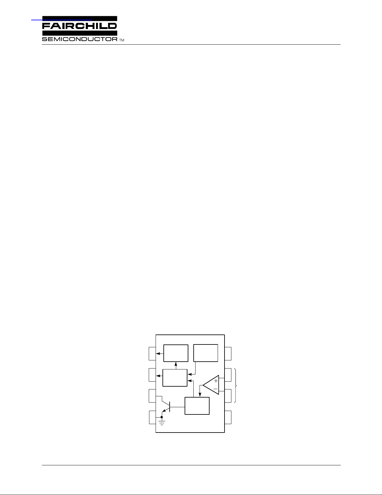
Functional Block Diagram
Switched
Current
Source Output
Switched
Reference
Output
Open Collector
Output
Ground
1
2
3
4
Switched
Current
Source
Switched
Voltage
Reference
Open Collector
Logic Output
Transistor
4152
Precision
One Shot
Voltage
Reference
Open Loop
Comparator
4152-01
8
7
6
5
-V
S
Comparator
Inputs
One Shot
Timing
Rev. 1.0.1
PRODUCT SPECIFICATION RC4152
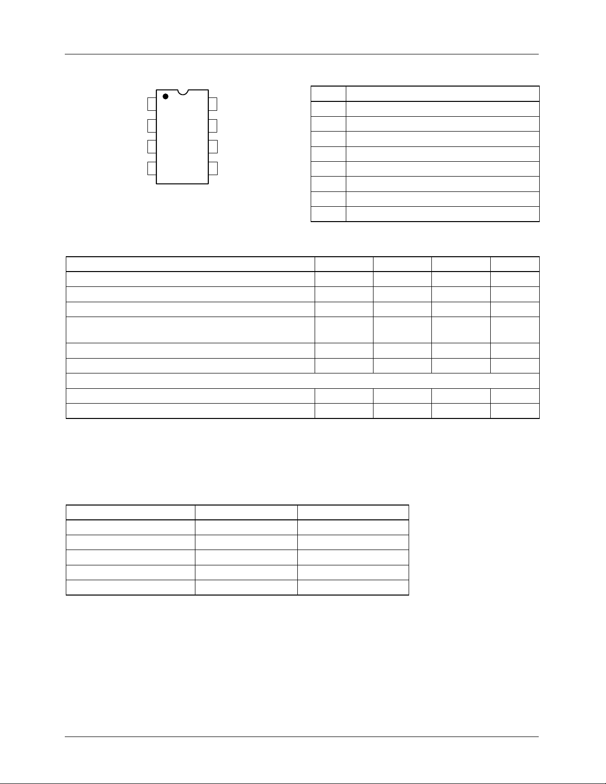
Pin Assignments Pin Descriptions
Pin Function
I
OUT
R
F
OUT
GND
1
2
S
3
4
8
7
6
5
4152-02
+V
V
V
C
S
IN
TH
O
1 Switched Current Source Output (I
2 Switched Voltage Reference (RS)
3 Logic Output (Open Collector) (F
4 Ground (GND)
5 One-Shot R, C Timing (CO)
OUT
6 Threshold (VTH)
7 Input Voltage (VlN)
8+V
S
Absolute Maximum Ratings
Parameter Min. Typ. Max. Units
Supply Voltage +22 V
Internal Power Dissipation 500 mW
Input Voltage -0.2 +V
Output Sink Current
(Frequency Output)
Output Short Circuit to Ground Continuous
Storage Temperature Range -65 +150 °C
Operating Temperature Range
RC4152 0 +70 °C
RV4152N -25 +85 °C
Note:
1. “Absolute maximum ratings” are those beyond which the safety of the device cannot be guaranteed. They are not meant to
imply that the device should be operated at these limits. If the device is subjected to the limits in the absolute maximum ratings
for extended periods, its reliability may be impaired. The tables of Electrical Characteristics provides conditions for actual
device operation.
S
20 mA
OUT
)
)
V
Thermal Characteristics
8-Lead Plastic DIP Small Outline SO-8
Max. Junction Temp. +125°C +125°C
Max. P
Therm. Res q
Therm. Res q
For TA>50°C Derate at 6.25 mW/°C 4.17mW/°C
2
<50°C 468 mW 300mW
D TA
JC
JC
——
160°C/W 240°C/W
RC4152 PRODUCT SPECIFICATION
Electrical Characteristics
(VS = +15V, and TA = +25°C unless otherwise noted)
Parameters Test Conditions Min. Typ. Max. Units
Power Supply Requirements (Pin 8)
Supply Current VS = +15V 2.5 6.0 mA
Supply Voltage +7.0 +15 +18 V
Input Comparator (Pins 6 and 7)
V
OS
Input Bias Current -50 -300 nA
Input Offset Current ±30 ±100 nA
Input Voltage Range 0 VS-2 VS-3 V
One Shot (Pin 5)
Threshold Voltage 0.65 0.67 0.69 V
Input Bias Current -50 -500 nA
Saturation Voltage I = 2.2 mA 0.1 0.5 V
Drift of Timing vs. Temperature
2
T = 75 ms over the specified
temperature range
Timing Drift vs. Supply Voltage ±100 ppm/V
Switched Current Source (pin 1)
1
Output Current RS = 16.7K +138 mA
Drift vs. Temperature
2
over specified temperature range ±50 ±100 ppm/°C
Drift vs. Supply Voltage 0.10 %/V
Leakage Current Off State 1.0 50 nA
Compliance Pin 1 = 0V to +10V 1.0 2.5 mA
Reference Voltage (Pin 2)
V
REF
Drift vs. Temperature
Logic output (Pin 3)
Saturation Voltage
2
over specified temperature range ±50 ±100 ppm/°C
I
= 3 mA 0.1 0.5 V
SINK
I
= 10 mA 0.8 V
SINK
2.0 2.25 2.5 V
Leakage Current Off State 0.1 1.0 mA
Nonlinearity Error
(Voltage Sourced Circuit of Figure 3) 1.0 Hz to 10 kHz 0.007 0.05 %
Temperature Drift Voltage2
(Voltage Sourced Circuit of Figure 3)
Notes:
1. Temperature coefficient of output current source (pin 1 output) exclusive of reference voltage drift.
2. Guaranteed but not tested.
F
= 10 kHz,
OUT
over specified temperature range ±75 ±150 ppm/°C
±2.0 ±10 mV
S
±30 ±50 ppm/°C
3
PRODUCT SPECIFICATION RC4152
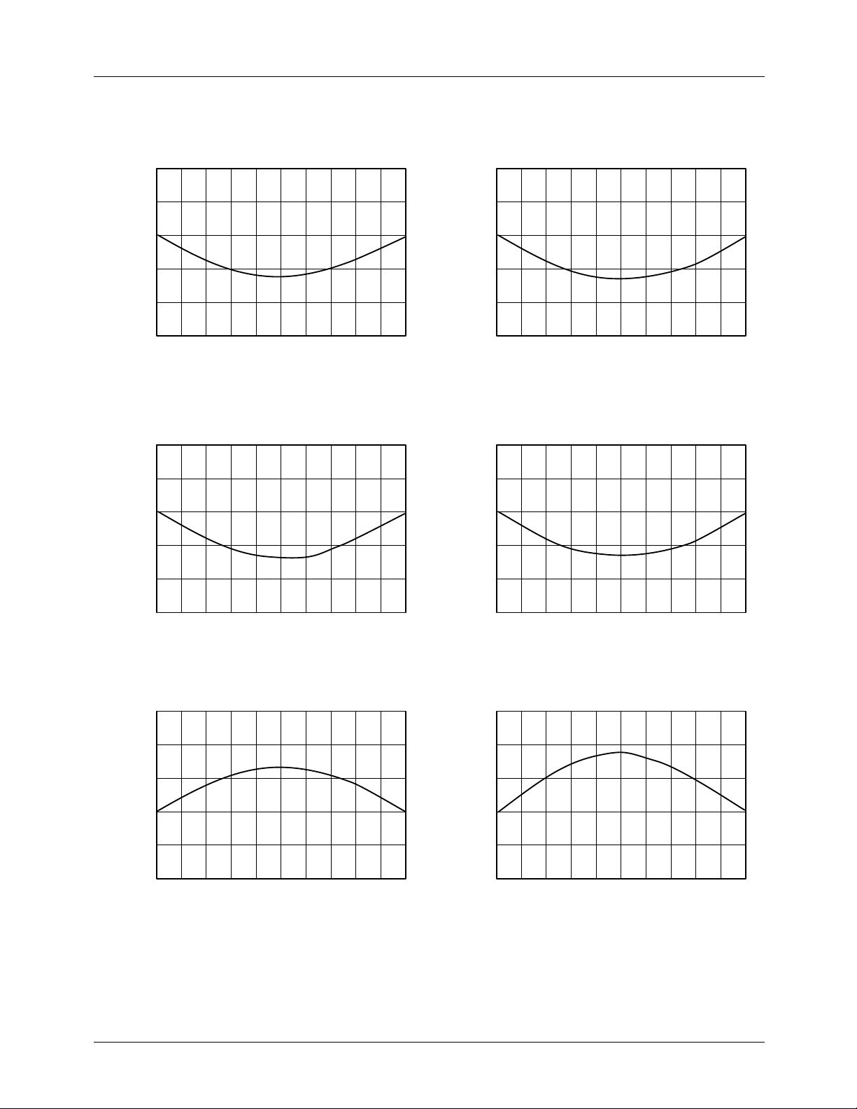
Typical Performance Characteristics
10 KHz Current-Sourced VFC
Nonlinearity vs. Input Voltage
+0.01
+0.005
0
-0.005
NL (% Error)
-0.01
-0.015
1
0
+0.01
+0.005
0
-0.005
NL (% Error)
-0.01
2345678910
(V)
V
IN
10 KHz Voltage-Sourced VFC
Nonlinearity vs. Input Voltage
+0.06
+0.03
0
-0.03
NL (% Error)
-0.06
-0.09
0
+0.10
+0.05
0
-0.05
NL (% Error)
-0.10
100 KHz Current-Sourced VFC
Nonlinearity vs. Input Voltage
1
2345678910
V
(V)
IN
100 KHz Voltage-Sourced VFC
Nonlinearity vs. Input Voltage
-0.015
0
+0.01
+0.005
0
-0.005
NL (% Error)
-0.01
-0.015
0
1
2345678910
(V)
V
IN
10 KHz Precision VFC
Nonlinearity vs. Input Frequency
1
2345678910
F
(kHz)
IN
-0.15
0
+0.12
+0.08
+0.04
0
NL (% Error)
-0.04
-0.08
0
1
2345678910
(V)
V
IN
100 KHz Precision VFC
Nonlinearity vs. Input Frequency
1
2345678910
F
(kHz)
IN
4152-03
4

RC4152 PRODUCT SPECIFICATION
Principles of Operation
The RC4152 contains the following components: an open
loop comparator, a precision one-shot timer, a switched voltage reference, a switched current source, and an open collector logic output transistor. These functional blocks are
internally interconnected. Thus, by adding some external
resistors and capacitors, a designer can create a complete
voltage-to-frequency converter.
The comparator’s output controls the one-shot (monostable
timer). The one-shot in turn controls the switched voltage
reference, the switched current source and the open collector
output transistor. The functional block diagram shows the
components and their interconnection.
To detail, if the voltage at pin 7 is greater than the voltage at
pin 6, the comparator switches and triggers the one-shot.
When the one-shot is triggered, two things happen. First, the
one-shot begins its timing period. Second, the one-shot’s
output turns on the switched voltage reference, the switched
current source and the open collector output transistor.
The one-shot creates its timing period much like the popular
555 timer does, by charging a capacitor from a resistor tied
to +VS. The one-shot senses the voltage on the capacitor
(pin 5) and ends the timing period when the voltage reaches
2/3 of the supply voltage. At the end of the timing period, the
capacitor is discharged by a transistor similar to the open
collector output transistor.
Meanwhile, during the timing period of the one-shot, the
switched current source, the switched voltage reference, and
the open collector output transistor all will be switched on.
The switched current source (pin 1) will deliver a current
proportional to both the reference and an external resistor,
RS. The switched reference (pin 2) will supply an output
voltage equal to the internal reference voltage (2.25V). The
open collector output transistor we be turned on, forcing the
logic output (pin 3) to a low state. At the end of the timing
period all of these outputs will turn off. The switched voltage
reference has produced an off-on-off voltage pulse, the
switched current source has emitted a quanta of charge, and
the open collector output has transmitted a logic pulse.
To summarize, the purpose of the circuit is to produce a current pulse, well-defined in amplitude and duration, and to
simultaneously produce an output pulse which is compatible
with most logic families. The circuit's outputs show a pulse
waveform in response to a voltage difference between the
comparators inputs.
Integrator
C
B
R
B
Current Setting Resistor
= 16.7K
R
S
R
LOAD
Open Collector Output
I
OUT
1
2
R
S
Ground
F
OUT
Reference
3
4
4152
Switched
Current
Source
Switched
Voltage
Open Collector
Logic Output
Transistor
Voltage
Reference
Open Loop
Comparator
Precision
One Shot
+V
O
O
100K
0.01 Fm
One Shot
Timing
S
V
IN
0 to +10V
4152-04
8
7
6
R
5
C
Figure 1. Single Supply VFC
5

PRODUCT SPECIFICATION RC4152
Applications
Single Supply VFC
The stand-alone voltage-to-frequency con v erter is one of the
simplest applications for the RC4152. This application uses
only passive external components to create the least expensive VFC circuit (see Figure 1).
The positive input voltage VIN is applied to the input comparator through a low pass filter. The one-shot will fire repetitively and the switched current source will pump out current
pulses of amplitude V
integrator. Because the inte grator is tied back to the in v erting
comparator input, a feedback loop is created. The pulse repetition rate will increase until the average voltage on the integrator is equal to the DC input voltage at pin 7. The average
voltage at pin 6 is proportional to the output frequency
because the amount of charge in each current pulse is
precisely controlled.
Because the one-shot firing frequency is the same as the
open collector output frequency, the output frequency is
directly proportional to VIN.
The external passive components set the scale factor. For
best linearity, RS should be limited to a range of 12 kW to
20 kW
and duration 1.1 ROCO into the
REF/RS
The reference voltage is nominally 2.25V for the RC4152.
Recommended values for different operating frequencies are
shown in the table below.
Operating
Range R
DC to 1.0 kHz 6.8 kW 0.1 mF 100 kW 10 mF
DC to 10 kHz 6.8 kW 0.01 mF 100 kW 10 mF
DC to 100 kHz 6.8 kW 0.001 mF 100 kW 10 mF
O
The single supply VFC is recommended for uses where
dynamic range of the input is limited, and the input does not
reach 0V. With 10 kHz values, nonlinearity will be less than
1.0% for a 10 mV to 10V input range, and response time will
be about 135 ms.
C
O
R
B
1
T
-------------=
F
OUT
V
-------------=
OUT
REF
R
S
T
P
------
where TP = 1.1 R
T
OCO
V
IN
------------ I
=
R
B
I
OUT
By rearranging and substituting,
F
OUT
=
V
IN
------------V
REF
S
------ -
---------------------- -
1.1R
R
B
1
C
O
O
R
Recommended component values for different operating
frequencies are shown in the table below.
Range
Input V
0 to -10V 0 to 1.0 kHz 0.1 KHz/V 6.8 kW 0.1 mF 0.05 mF 100 kW
0 to -10V 0 to 10 kHz 1.0 KHz/V 6.8 kW 0.01 mF 0.005 mF 100 kW
0 to -10V 0 to 100 kHz 10 KHz/V 6.8 kW 0.001 mF 500 pF 100 kW
Output
F
IN
O
Scale
Factor R
C
O
C
O
R
I
B
The graphs shown under Typical Performance Characteristics show nonlinearity versus input voltage for the precision
current sourced VFC. The best linearity is achieved by using
an op amp having greater than 1.0 V/ ms sle w rate, b ut an y op
amp can be used.
Precision V oltage Sourced VFC
This circuit is identical to the current sourced VFC, except
that the current pulses into the integrator are derived directly
C
B
from the switched voltage reference. This improves temperature drift at the expense of high frequency linearity.
The switched current source (pin 1) output has been tied to
ground, and RS has been put in series between the switched
voltage reference (pin 2) and the summing node of the op
amp. This eliminates temperature drift associated with the
switched current source. The graphs under the Typical
Performance Characteristics show that the nonlinearity error
is worse at high frequency, when compared with the current
sourced circuit.
Precision Current Sourced VFC
This circuit operates similarly to the single supply VFC,
except that the passive R-C integrator has been replaced by
an active op amp integrator. This increases the dynamic
range down to 0V, improves the response time, and
eliminates the nonlinearity error introduced by the limited
compliance of the switched current source output.
The integrator algebraically sums the positive current pulses
from the switched current source with the current VIN/RB.
To operate correctly, the input voltage must be negative, so
that when the circuit is balanced, the two currents cancel.
6
Single Supply FVC
A frequency-to-voltage converter performs the exact opposite of the VFCs function; it con verts an input pulse train into
an average output voltage. Incoming pulses trigger the input
comparator and fire the one-shot. The one-shot then dumps a
charge into the output integrator. The voltage on the integrator becomes a varying DC voltage proportional to the
frequency of the input signal. Figure 4 shows a complete
single supply FVC.

RC4152 PRODUCT SPECIFICATION
C
I
m
0.005 F
1N914
-V
S
+V
S
2
3
1
R
100 k W
+V
S
V
IN
OP-27
B+
8
74
+V
S
4
10k
R
+V
7
L
W
+V
S
6
8
Offset
Adjust
S
10 kW
m
1 F
100
W
4152-05
+V
L
R
L
5.1K
F
OUT
Output Frequency
0 F 10kHz
O
V
IN
0 to -10V
R = 16.7K
S
3
F
OUT
Gnd
C
O
0.01 F
R
B
100K
2
1
I
R
OUT
S
4152
VFC
C
5
V
O
TH
6
5k
W
m
R
O
6.8 k W
Figure 2. Precision Current Sourced VFC
0 to -10V
+V
R
5.1K
F
OUT
Output Frequency
0 F 10kHz
OUT
C
I
0.005 F
1N914
-V
S
+V
V
L
IN
L
R
B
100K
R = 16.7K
S
2
3
R
B+
100 k
+V
OP-27
1
W
S
4
R
10k
+V
7
Z
W
S
21
3
F
OUT
4
Gnd
C
O
m
0.01 F
RI
OUT
S
4152
VFC
C
5
V
O
6
8
+V
S
7
V
IN
TH
5 kW
+V
R
O
6.8 k W
S
Figure 3. Precision Voltage Sourced VFC
m
S
6
8
Offset
Adjust
10 kW
m
1 F
100
W
4152-06
7

PRODUCT SPECIFICATION RC4152
The input waveform must have fast slewing edges, and the
differentiated input signal must be less than the timing
period of the one-shot, 1.1 ROCO. A differentiator and
divider are used to shape and bias the trigger input; a negative going pulse at pin 6 will cause the comparator to fire the
one-shot. The input pulse amplitude must be large enough to
trip the comparator, but not so large as to exceed the ICs
input voltage ratings.
The output voltage is directly proportional to the input
frequency:
V
OUT
1.1ROCORBV
-------------------------------------------- -
REF
F
Hz()=
R
S
IN
Output ripple can be minimized by increasing CB, but this
will limit the response time. Recommended values for
various operating ranges are shown in the following table.
Input
Operating
Rage C
0 to 1.0 kHz 0.02 mF 6.8 kW 0.1 mF 100 kW 100 mF 1.0 mV
0 to 10 kHz 0.002 mF 6.8 kW 0.01 mF 100 kW 10 mF 1.0 mV
0 to 100 kHz 200 pF 6.8 kW 0.001 mF 100 kW 1.0 mF 1.0 mV
R
IN
C
O
R
O
B
CBRipple
Precision FVC
Linearity, offset and response time can be improved by
adding one or more op amps to form an active lowpass filter
at the output. A circuit using a single pole acti v e integrator is
shown in Figure 5.
The positive output current pulses are av eraged by the inverting integrator, causing the output voltage to be negative.
Response time can be further improved by adding a double
pole filter to replace the single pole filter. Refer to the graphs
under Typical Performance Characteristics that show
nonlinearity error versus input frequency for the
precision FVC circuit.
+15V
C
IN
m
0.022 F
F
IN
Frequency
Input
0 F 10kHz
IN
10 k
10 k
W
Ÿ
W
10 k
7
V
6
V
TH
+V
W
5 k
W
+15V
100K
Figure 4. Single Supply FVC
IN
R
R
O
W
6.8 k
5
C
O
V
OUT
C
B
m
10 F
Gnd
F
R
OUT
S
2
4152
VFC
I
OUT
S
1
8
B
C
0.01 F
4
3
R = 16.7K
S
O
m
4152-07
8

RC4152 PRODUCT SPECIFICATION
R
O
6.8 k
W
+15V
10 k
W
W
C
IN
m
0.022 F
F
IN
Frequency Input
0 F 10kHz
O
5.0 V
P-P
Squarewave
10 k
10 k
6
5 k
V
W
TH
W
+15V
7
V
IN
4152 VFC
+V
S
8
I
OUT
C
R
5
O
Gnd
F
OUT
S
21
R = 16.7K
S
C
O
m
0.01 F
4
3
R
C
I
B
100 k
W
5 pF
-V
S
+V
R
B
100 k
4
2
OP-27
3
1
W
10 k
R
S
7
8
Z
W
6
Offset
Adjust
100
W
V
OUT
Voltage Output
-10V V 0
O
+V
S
4152-08
9

PRODUCT SPECIFICATION RC4152
+V
S
(8)
Q36
Q37
Q35
Q33
Q34
3.6K
I
OUT
(1)
R
S
(2)
Q28
15K
Q41
Q27
Q26
7.8K
Q25
Q4
Q3
Q2
Q1
(6)
V
TH
IN
V
(7)
Q5
Q6
Q7
Q8
2K
2K
Q9
Q10
Q11
2K
2K
Q21
2K
2K
Q22
Q23
Q17
Q16 Q18
Q12
Q13
(5)
C
O
Q14
Q19 Q20
Gnd
(4)
10K
10K
10K
-V
S
Q15
12K
D39
D43
Q42
Q38
Q40
W
V
U
TX
(3)
F
o
UT
Q32
D29
6.3V
S
RY
N
ZM
4152-09
Q30
6.2K
2K
Schematic Diagram
10

RC4152 PRODUCT SPECIFICATION
Notes:
11

PRODUCT SPECIFICATION RC4152
Ordering Information
Part Number Package Operating Temperature Range
RC4152N N 0°C to +70°C
RC4152M M 0°C to 70°C
RV4152N N -25°C to +85°C
Notes:
N = 8-lead plastic DIP
M = 8-lead plastic SOIC
LIFE SUPPORT POLICY
FAIRCHILD’S PRODUCTS ARE NOT AUTHORIZED FOR USE AS CRITICAL COMPONENTS IN LIFE SUPPORT DEVICES
OR SYSTEMS WITHOUT THE EXPRESS WRITTEN APPROVAL OF THE PRESIDENT OF FAIRCHILD SEMICONDUCTOR
CORPORATION. As used herein:
1. Life support devices or systems are devices or systems
which, (a) are intended for surgical implant into the body,
or (b) support or sustain life, and (c) whose failure to
perform when properly used in accordance with
instructions for use provided in the labeling, can be
reasonably expected to result in a significant injury of the
user.
2. A critical component in any component of a life support
device or system whose failure to perform can be
reasonably expected to cause the failure of the life support
device or system, or to affect its safety or effectiveness.
www.fairchildsemi.com
6/25/98 0.0m 003
Ó 1998 Fairchild Semiconductor Corporation
Stock#DS30004152
 Loading...